

TPS2553QDBVRQ1 Automotive USB Power Switch: Specs, Design & Applications
A practical engineering guide to the Texas Instruments TPS2553QDBVRQ1, covering adjustable current limiting, 2.5 V to 6.5 V operation, an 85 mΩ high-side MOSFET, reverse-voltage blocking, fault reporting, SOT-23 pinout, automotive design considerations and replacement selection.
What Is TPS2553QDBVRQ1?
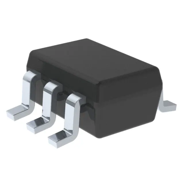
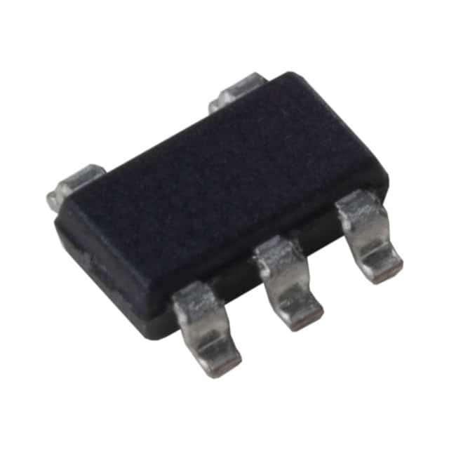
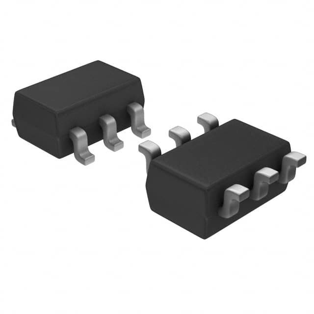
TPS2553QDBVRQ1 is an automotive-qualified, single-channel precision current-limited power-distribution switch from Texas Instruments. It combines an integrated low-resistance high-side MOSFET with an adjustable current limit, active-high enable control, built-in soft-start, active-low fault reporting and reverse-voltage protection. The device operates from 2.5 V to 6.5 V and is supplied in a compact 6-pin SOT-23 DBV package. It is especially useful for automotive USB ports and other low-voltage loads that must be protected against overloads, short circuits and excessive inrush current.
TPS2553QDBVRQ1 Key Specifications
The TPS2553QDBVRQ1 belongs to the TPS2553-Q1 family of precision current-limited power-distribution switches. Its purpose is not simply to turn a power rail on and off. It actively supervises the current flowing from the source to the load and responds when that current exceeds a programmed limit.
This makes the device more useful than a basic discrete MOSFET in systems where cables, connectors, USB ports or external accessories may be exposed to overloads, damaged loads or short circuits.
| Parameter | TPS2553QDBVRQ1 | Engineering Meaning |
|---|---|---|
| Manufacturer | Texas Instruments | Automotive power-management IC |
| Product Family | TPS2553-Q1 | Precision current-limited power-distribution switch |
| Channels | 1 | Controls one protected power output |
| Input Voltage | 2.5 V to 6.5 V | Suitable for common low-voltage power rails |
| Current Limit | 75 mA to 1.3 A typical adjustable range | External resistor programs the protection threshold |
| Maximum Load Current | Up to 1.5 A | Defines device load-current capability under specified conditions |
| Integrated MOSFET | 85 mΩ | Low resistance helps reduce conduction loss |
| Enable Logic | Active High | Logic high enables the power path |
| Overcurrent Response | Approximately 2 µs typical | Fast response helps protect the upstream supply and wiring |
| Fault Output | Active-Low Open-Drain | Allows a controller to detect protection events |
| Reverse Protection | Yes | Helps prevent reverse current from OUT toward IN |
| Soft-Start | Integrated | Reduces turn-on current surge |
| Automotive Qualification | AEC-Q100 | Designed and qualified for automotive applications |
| Operating Temperature | -40°C to +125°C | AEC-Q100 Grade 1 temperature range |
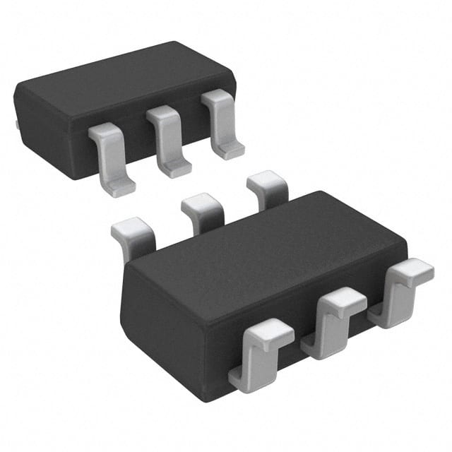
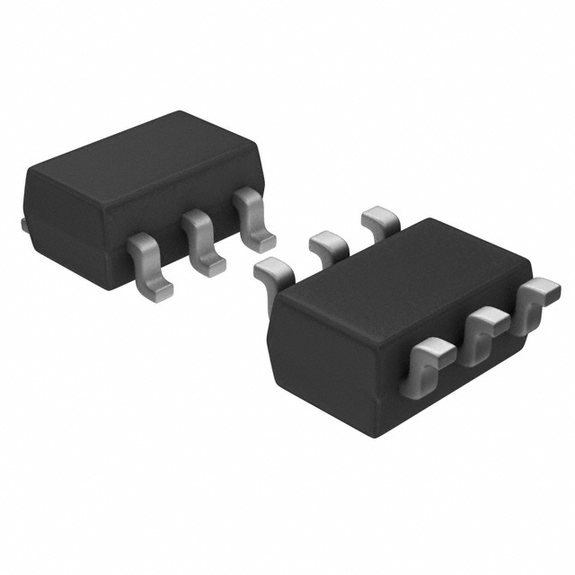
| Package | SOT-23 / DBV | Compact 6-pin surface-mount package |
| Ordering Part Number | TPS2553QDBVRQ1 | Automotive DBV tape-and-reel version |
A useful design distinction is that the adjustable current-limit range and the maximum load-current rating are not the same specification. Engineers should not treat the 1.5 A load-current figure as though it were simply a 1.5 A programmable current-limit setting.
Understanding the TPS2553QDBVRQ1 Part Number
The full ordering code provides information that helps purchasing teams and engineers distinguish the exact device from related TPS2553 variants.
Identifies the precision adjustable current-limited power-distribution switch family.
Identifies the automotive-qualified version intended for applications requiring AEC-Q100 qualification.
Identifies the 6-pin DBV SOT-23 package supplied in tape-and-reel packaging.
When ordering components, use the complete TPS2553QDBVRQ1 part number rather than shortening the purchase description to TPS2553. Similar members of the family can have different enable polarity, qualification level, current behavior or packaging.
How the TPS2553QDBVRQ1 Works
At the center of the TPS2553QDBVRQ1 is an integrated high-side N-channel power MOSFET. When the EN input is asserted high, internal circuitry turns on this MOSFET and connects the IN supply to the OUT pin.
Under normal operating conditions the device behaves like a low-resistance electronic switch. The integrated MOSFET has approximately 85 mΩ on-resistance under the relevant specified conditions, helping reduce the voltage drop between input and output.
The important difference appears when the load demands too much current. Instead of allowing current to increase without control, the TPS2553QDBVRQ1 measures the load current internally and enters a constant-current limiting condition when the programmed threshold is exceeded.
This behavior can protect PCB traces, connectors, cables and upstream power converters from an uncontrolled overload.
The internal MOSFET is on and power flows from IN to OUT with a relatively small voltage drop.
Internal control circuitry regulates the load current rather than allowing it to rise freely.
The active-low FAULT output can inform a microcontroller that an abnormal operating condition has occurred.
Adjustable Current Limit and the ILIM Pin
One of the strongest reasons to select the TPS2553QDBVRQ1 automotive power switch is its adjustable current-limit threshold.
The ILIM pin allows an external resistor to define the current level at which the protection circuit begins regulating the output. This gives designers much greater flexibility than a fixed-current protection switch.
For example, two products may use the same 5 V source but have very different safe load-current limits. A low-power sensor interface may need a conservative limit, while an automotive USB accessory port may require a substantially higher threshold. The same IC family can support both design goals by changing the ILIM resistor.
The datasheet specifies a recommended ILIM resistor range, so resistor selection should follow the current-limit equations and design curves published for the TPS2553-Q1 rather than using an arbitrary resistor. Component tolerance should also be included in the worst-case current calculation.
Why Current-Limit Accuracy Matters
A poorly controlled current threshold creates two opposite problems. If the threshold is too low, a valid load may trip protection during normal startup. If the threshold is too high, the connector, cable, power supply or downstream circuit may experience more current than intended during a fault.
For this reason, the designer should evaluate current-limit tolerance together with load-current tolerance, temperature, component variation and startup surge current.
Do not design the normal continuous load current exactly at the current-limit threshold. Practical systems need operating margin so normal load variation does not look like a fault.
Overcurrent and Short-Circuit Protection
A USB or external accessory connector is one of the easiest places for an electronic product to experience unpredictable electrical conditions. Users may connect damaged cables, defective accessories or loads containing large capacitors.
The TPS2553QDBVRQ1 is designed for exactly this type of environment. When current rises above the programmed threshold, the device responds quickly and regulates the current rather than allowing the load to pull unlimited current from the source.
Texas Instruments specifies a typical fast overcurrent response on the order of microseconds. Fast response matters because even a short fault can collapse a shared supply rail or produce a large transient in wiring with low impedance.
If the abnormal load causes excessive device heating, internal thermal protection provides another protection layer. The FAULT output can also inform the main controller that intervention or user notification may be required.
Constant-Current Protection vs Immediate Latch-Off
The TPS2553-Q1 uses a constant-current protection approach during overload. That means the device attempts to regulate current around its limit instead of immediately becoming a permanently latched-off switch after the first overcurrent event.
This behavior can be useful for loads with temporary startup surges. However, engineers must still analyze fault power dissipation because limiting current does not mean the switch dissipates zero power.
TPS2553QDBVRQ1 Pinout and Pin Functions
The TPS2553QDBVRQ1 uses a compact 6-pin SOT-23 DBV package. Its simple pinout makes the part relatively easy to integrate into space-constrained power-distribution circuits.
| Pin | Name | Function |
|---|---|---|
| 1 | IN | Power input. Use local ceramic bypass capacitance close to IN and GND. |
| 2 | GND | Ground reference for the control and protection circuitry. |
| 3 | EN | Active-high enable input. A logic-high signal enables the power switch. |
| 4 | FAULT | Active-low open-drain fault output for overcurrent, overtemperature and reverse-voltage conditions. |
| 5 | ILIM | Connects to an external resistor used to program the current-limit threshold. |
| 6 | OUT | Protected power-switch output connected to the load. |
Because FAULT is an open-drain output, it normally requires an external pull-up resistor to an appropriate logic rail. This also allows fault reporting to interface conveniently with many microcontrollers.
Using the FAULT Output Effectively
The FAULT signal should not be treated as a decorative status pin. It can become an important part of system-level diagnostics.
A vehicle controller can monitor FAULT and record whether a downstream port experienced an overload, excessive temperature or reverse-voltage event. Firmware can then decide whether to retry the output, disable a related subsystem, store a diagnostic code or notify the user.
In a robust design, the software response should distinguish between a temporary event and a persistent problem. For example, a brief capacitive startup event may not require the same response as a hard short that remains present for many seconds.
This combination of hardware current limiting and software supervision is often more useful than relying only on a fuse, because the controller gains information about what happened.
Why Reverse-Voltage Blocking Matters
Reverse-current behavior is an important feature in systems where the output node can be powered from another source.
If OUT rises above IN, an ordinary high-side switch may allow unwanted current to flow back toward the source. In a USB or automotive system, that current can back-power a regulator, another PCB rail or equipment that is supposed to be turned off.
The TPS2553QDBVRQ1 includes reverse input-output voltage protection. Internal circuitry detects the reverse condition and disables the power switch to help protect the upstream side.
This is one of the meaningful improvements when the TPS2553-Q1 is evaluated as an upgrade from some older power-distribution switch designs.
Reverse blocking is not only a protection specification. It can prevent unexpected power-state behavior, difficult startup sequences and back-powered circuits that are extremely confusing during system debugging.
Soft-Start and Capacitive Load Management
A downstream USB port or accessory circuit often contains significant capacitance. When an uncharged capacitor is suddenly connected to a power rail, it initially behaves almost like a short circuit.
Without controlled turn-on, this inrush current can cause a supply dip, connector stress or an unwanted system reset.
The TPS2553QDBVRQ1 controls its output rise behavior and includes soft-start functionality. This helps reduce the sudden current surge associated with charging downstream capacitance.
However, soft-start does not remove the need for proper system design. The engineer should still check the source impedance, load capacitance, USB requirements where applicable, current-limit setting and upstream converter response.
A power switch can control the connection, but the complete power path still includes the cable, PCB copper, capacitors, regulator and load. All of those components influence startup behavior.
Understanding the 85 mΩ On-Resistance
The integrated high-side MOSFET is specified with low on-resistance, which is important for both voltage drop and heat generation.
A simplified conduction-loss estimate can be obtained using:
P ≈ I² × R
For example, as load current increases, conduction loss rises with the square of current. This is why a small resistance value can still become thermally important in a compact SOT-23 package at higher load currents.
The voltage delivered to the load is also slightly lower than the source voltage because current flowing through the MOSFET creates a voltage drop. In many USB-style systems that drop is small, but it should still be included in worst-case voltage budgeting.
Engineers should also remember that MOSFET resistance changes with temperature and production variation. A room-temperature typical value is not a replacement for the worst-case values and curves in the datasheet.
TPS2553QDBVRQ1 for Automotive Applications
The Q1 qualification is one of the most important differences between TPS2553QDBVRQ1 and a general-purpose USB power switch. The device is qualified for automotive applications and supports an ambient operating temperature range from -40°C to +125°C.
Automotive electronics must operate through temperature extremes, long service life, electrical transients and widely varying operating conditions. The power switch is therefore often part of a larger protection architecture rather than the only protection component.
Protect USB power rails used by phones, storage devices and other connected accessories.
Control protected low-voltage outputs connected to communication and accessory electronics.
Add programmable current limiting to external or removable low-voltage loads.
AEC-Q100 qualification does not mean the device can be connected directly to every vehicle battery rail. The TPS2553QDBVRQ1 has a 2.5 V to 6.5 V operating range, so automotive systems normally use it downstream from a regulated low-voltage supply.
Common TPS2553QDBVRQ1 Applications
Although the part is often described as an automotive USB power switch, its function is broader. It can be used anywhere a low-voltage load requires an electronically controlled high-side switch with accurate current limiting.
- Automotive USB power ports
- Infotainment systems
- Telematics modules
- Protected accessory power rails
- USB hubs and downstream ports
- Navigation electronics
- Display and HMI systems
- Low-voltage sensor power distribution
- Embedded computing systems
- Protected peripheral interfaces
- Capacitive-load switching
- Short-circuit protected power outputs
The key selection question is not whether the application contains the letters "USB." The more useful question is whether the design needs a 2.5 V to 6.5 V high-side output that can be enabled digitally, limited to a controlled current and monitored for fault conditions.
PCB Layout Guidelines for TPS2553QDBVRQ1
The device is easy to connect schematically, but layout still determines how well the complete power path behaves.
The input bypass capacitor should be located close to the IN and GND pins. The high-current path from the source through IN, through the switch and from OUT to the load should use short, low-resistance copper paths.
- Place the input ceramic capacitor close to IN and GND.
- Keep the IN and OUT power traces short and sufficiently wide.
- Avoid narrow neck-down regions in the main current path.
- Keep the ILIM resistor close to the device.
- Route ILIM away from noisy switching nodes where practical.
- Provide a correct pull-up for the open-drain FAULT output.
- Keep the ground reference clean and low impedance.
- Evaluate copper area when estimating thermal performance.
- Check connector and cable resistance in the total voltage-drop budget.
- Measure startup and fault waveforms on production-like hardware.
A precision current-limited switch can only control the current it senses internally. Poor PCB copper, connector resistance and cable resistance are outside the IC and still influence the voltage actually delivered to the load.
Thermal Design and Fault Power
Because the TPS2553QDBVRQ1 contains the power MOSFET inside a small SOT-23 package, thermal analysis is important when load current is high or when an overload persists.
During normal operation, dissipation is dominated mainly by the load current and MOSFET resistance. During current limiting, the situation can be much more demanding because the switch may simultaneously carry substantial current and drop significant voltage.
For example, a shorted or partially shorted output may force the device to regulate current while much of the input voltage appears across the power switch. This creates considerably more dissipation than normal low-resistance operation.
Thermal shutdown provides protection against dangerous internal temperature, but it should not be treated as a normal operating method. A well-designed product should evaluate expected overload duration, ambient temperature, PCB copper, enclosure temperature and retry behavior.
TPS2553QDBVRQ1 vs TPS2551QDBVRQ1
Engineers maintaining an older design may encounter the TPS2551QDBVRQ1. The two devices are related, but the TPS2553-Q1 provides important improvements and is listed by Texas Instruments as a compatible upgrade path for the older TPS2551-Q1 family.
| Feature | TPS2553QDBVRQ1 | TPS2551QDBVRQ1 |
|---|---|---|
| Automotive Qualification | Yes | Yes |
| Enable | Active High | Active High |
| Input Voltage | 2.5 V to 6.5 V | 2.5 V to 6.5 V |
| Integrated Switch | 85 mΩ class | 85 mΩ class |
| Current-Limit Capability | Expanded / improved precision range | Older implementation |
| Reverse Blocking | Integrated reverse-voltage protection | Check original design requirements |
| Lifecycle Direction | Active | Not recommended for new designs |
For a new design, TPS2553QDBVRQ1 is generally the more logical part to evaluate. For an existing PCB, designers should still compare the complete datasheets, current-limit resistor calculation, timing, fault behavior and worst-case electrical characteristics before changing production hardware.
TPS2553QDBVRQ1 Replacement and Equivalent Selection
A search for a TPS2553QDBVRQ1 replacement should not be reduced to finding another 6-pin power switch with approximately the same current rating.
The replacement must match both electrical behavior and system behavior. Two power switches may have the same voltage and current ratings but react very differently during startup, short circuit or reverse-voltage events.
| Replacement Check | TPS2553QDBVRQ1 Reference | Why It Matters |
|---|---|---|
| Input Voltage | 2.5 V to 6.5 V | Replacement must support the full regulated rail range |
| Enable Polarity | Active High | Wrong polarity can invert system power control |
| Current Limit | Adjustable | Programming method and accuracy must fit the original design |
| On-Resistance | 85 mΩ class | Affects voltage drop and thermal dissipation |
| Fault Output | Active-Low Open-Drain | Controller interface must remain compatible |
| Overload Behavior | Constant-current limiting | Different behavior can change system recovery |
| Reverse Blocking | Supported | Important when OUT can be externally powered |
| Qualification | Automotive / AEC-Q100 | Required for many automotive BOMs |
| Package | 6-pin SOT-23 DBV | Pinout and footprint must physically match |
| Temperature | -40°C to +125°C | Replacement must satisfy environmental requirements |
For automotive production, qualification status and traceability may be just as important as the electrical specification. A catalog-grade device with similar values is not automatically a valid substitute for a Q1 part.
Common TPS2553QDBVRQ1 Design Mistakes
Setting the Current Limit Too Close to Normal Load Current
Normal loads vary with temperature, operating mode and startup state. A threshold with no margin may produce nuisance faults even though the system is healthy.
Ignoring Cable and Connector Voltage Drop
The IC may have low internal resistance, but the external connector and cable can contribute much more resistance than the switch itself. Always calculate the complete power path.
Using FAULT Without the Correct Pull-Up
Because FAULT is an open-drain output, it requires an appropriate pull-up arrangement. Treating it as a push-pull logic output can lead to unreliable fault detection.
Assuming AEC-Q100 Means Direct Battery Connection
Automotive qualification does not change the input-voltage rating. TPS2553QDBVRQ1 operates on a regulated 2.5 V to 6.5 V rail rather than directly from the full vehicle battery environment.
Ignoring Power Dissipation During Current Limiting
A current-limited output can still produce substantial IC dissipation during a short circuit. Protection behavior and thermal cycling should be tested at the highest relevant ambient temperature.
Selecting a Replacement Only by Package
Matching the SOT-23 footprint is not enough. Current-limit behavior, enable polarity, FAULT logic and reverse-blocking function can all affect the system.
How to Source TPS2553QDBVRQ1 Safely
Automotive components are often purchased for long production cycles, service inventory and repair programs. That makes part-number accuracy and traceability especially important.
- Confirm the exact TPS2553QDBVRQ1 ordering code.
- Do not use the marketing title as the SKU or MPN.
- Verify Texas Instruments as the manufacturer.
- Confirm the DBV 6-pin SOT-23 package.
- Check Q1 automotive qualification requirements.
- Review lot and date-code requirements.
- Request traceability when required by the project.
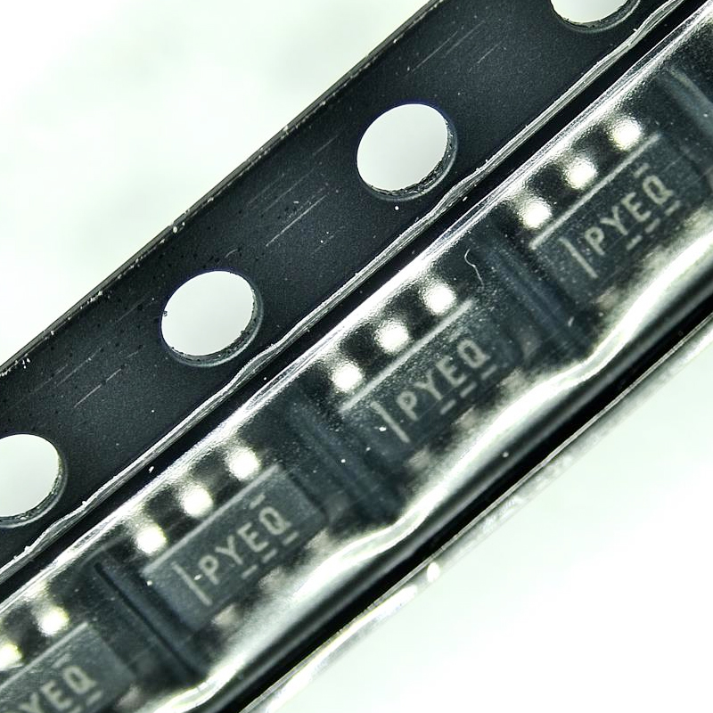
- Inspect reel and package markings.
- Verify moisture-sensitivity handling requirements.
- Review the latest manufacturer lifecycle status.
For database and structured-data purposes, the cleanest identifiers are: SKU: TPS2553QDBVRQ1 and MPN: TPS2553QDBVRQ1. Do not append descriptions such as "Automotive USB Power Switch SOT-23" to the SKU or MPN field.
TPS2553QDBVRQ1 FAQ
What is TPS2553QDBVRQ1?
TPS2553QDBVRQ1 is a Texas Instruments automotive precision current-limited power-distribution switch. It integrates a high-side MOSFET, adjustable current limiting, active-high enable, fault reporting, soft-start and reverse-voltage protection in a 6-pin SOT-23 package.
What is the input voltage range of TPS2553QDBVRQ1?
The TPS2553-Q1 operates from approximately 2.5 V to 6.5 V. It is intended for regulated low-voltage power rails rather than direct connection to a full automotive battery supply.
What is the TPS2553QDBVRQ1 current limit?
The device provides an adjustable current-limit function programmed by an external resistor connected to the ILIM pin. The TPS2553-Q1 product range is commonly specified from approximately 75 mA to 1.3 A for the adjustable current-limit range.
How much load current can TPS2553QDBVRQ1 handle?
Texas Instruments specifies the TPS2553-Q1 for up to approximately 1.5 A maximum load current under the relevant datasheet conditions. The maximum load-current specification should not be confused with the programmable current-limit range.
Is TPS2553QDBVRQ1 automotive qualified?
Yes. TPS2553QDBVRQ1 is an automotive Q1 device and is AEC-Q100 qualified. Its specified ambient operating temperature range extends from -40°C to +125°C.
Is the TPS2553QDBVRQ1 enable pin active high?
Yes. The EN pin is active high. Driving EN to a valid high logic level enables the internal power switch.
What does the FAULT pin do?
FAULT is an active-low open-drain output. It can report abnormal conditions such as overcurrent, overtemperature and reverse-voltage events to a microcontroller or other control circuit.
Does TPS2553QDBVRQ1 support reverse-current protection?
Yes. The device includes reverse input-output voltage protection. When the output voltage is driven above the input, internal circuitry can disable the switch to help prevent unwanted reverse current toward the input supply.
What package does TPS2553QDBVRQ1 use?
TPS2553QDBVRQ1 uses the Texas Instruments DBV package, a compact 6-pin SOT-23 surface-mount package.
What are the TPS2553QDBVRQ1 pins?
The six pins are IN on pin 1, GND on pin 2, EN on pin 3, FAULT on pin 4, ILIM on pin 5 and OUT on pin 6.
What is the on-resistance of TPS2553QDBVRQ1?
The TPS2553-Q1 family uses an integrated high-side MOSFET in the approximately 85 mΩ class under the relevant specified operating conditions. Actual resistance depends on temperature and operating conditions.
Can TPS2553QDBVRQ1 protect against a short circuit?
Yes. When load current exceeds the programmed threshold, the device uses constant-current limiting to restrict the current. Thermal protection and FAULT reporting provide additional system protection.
Can TPS2553QDBVRQ1 replace TPS2551QDBVRQ1?
TPS2553-Q1 is related to and backward compatible with the older TPS2551-Q1 family in relevant applications, but engineers should still compare pinout, current-limit resistor values, fault behavior, electrical limits and production requirements before approving a replacement.
Is TPS2553QDBVRQ1 suitable only for USB applications?
No. USB power distribution is a major application, but the device can also protect other 2.5 V to 6.5 V loads that require a controlled high-side switch, adjustable current limiting and fault monitoring.
What should be checked before using TPS2553QDBVRQ1?
Check input voltage, expected normal load current, ILIM resistor selection, startup current, load capacitance, PCB resistance, thermal conditions, FAULT pull-up voltage, reverse-power conditions and the latest Texas Instruments datasheet.
Final Engineering Perspective
The TPS2553QDBVRQ1 is more than a simple electronic on/off switch. Its value comes from combining power switching, programmable current protection, fault reporting, soft-start and reverse-current protection inside a small automotive-qualified package.
For USB ports and other externally accessible loads, these functions solve several problems at the same time. The switch controls power during normal use, limits current during overloads, helps reduce inrush current, reports faults to the system controller and helps prevent an externally powered output from feeding current backward into the source.
Its 2.5 V to 6.5 V operating range makes it suitable for common regulated 3.3 V and 5 V architectures, while the Q1 qualification makes it relevant to infotainment, telematics, HMI and other automotive electronic systems.
The most important design decision is not simply whether the part can carry the expected current. Engineers should choose the ILIM resistor with suitable margin, evaluate voltage drop through the complete wiring path, calculate heat under both normal and fault conditions, and verify the behavior of EN and FAULT within the overall control strategy.
For a new automotive design that requires an active-high protected low-voltage output with adjustable current limiting and reverse blocking, TPS2553QDBVRQ1 offers a compact and practical solution. Final component selection should always be confirmed against the latest Texas Instruments datasheet and the real electrical conditions of the application.