

APT40N60JCU2 600V MOSFET Power Module: Specs, Design & Applications
Explore APT40N60JCU2 specifications, Super Junction MOSFET technology, SOT-227 ISOTOP packaging, boost chopper operation, gate-drive design, thermal management, PFC applications, replacement selection and sourcing.
What Is APT40N60JCU2?
APT40N60JCU2 is a high-voltage N-channel Super Junction MOSFET power module originally developed by the Microsemi / Advanced Power Technology product family. It combines a 600 V drain-source voltage rating, 40 A continuous drain-current capability under specified case-temperature conditions, low 70 mΩ maximum on-resistance and an isolated SOT-227 / ISOTOP power package. Its boost-chopper configuration makes it especially relevant to PFC, switched-mode power supplies, motor control, braking circuits and other high-power switching systems.
APT40N60JCU2 Key Specifications
The APT40N60JCU2 is best understood as a complete power-switching module rather than as an ordinary small MOSFET. Its voltage rating, current capability, on-state resistance, gate characteristics, thermal performance and package design all work together to determine how the device behaves inside a real converter.
For engineers searching for an APT40N60JCU2 datasheet, the first step should be to understand what the main ratings actually mean in practical operation. A voltage or current number alone cannot describe the complete operating envelope of a power semiconductor.
| Parameter | APT40N60JCU2 | Engineering Meaning |
|---|---|---|
| Technology | Super Junction N-Channel MOSFET | Designed for efficient high-voltage switching |
| Configuration | Boost Chopper Module | Useful in PFC and boost-converter stages |
| Drain-Source Voltage | 600 V | Supports high-voltage DC-bus designs |
| Continuous Drain Current | 40 A at Tc = 25°C | High-current switching capability |
| Drain Current at Tc = 80°C | 30 A | Shows current derating with temperature |
| Pulsed Drain Current | 120 A | Relevant to short switching and transient events |
| Maximum RDS(on) | 70 mΩ | Important for conduction-loss calculations |
| Gate-Source Voltage | ±20 V | Absolute gate-voltage boundary |
| Total Gate Charge | 259 nC typical | Influences gate-driver requirements |
| Input Capacitance | 7015 pF typical | Influences switching behavior |
| Maximum Power Dissipation | 290 W at Tc = 25°C | Must be interpreted with thermal resistance |
| Junction Temperature | -55°C to +150°C | Defines the junction operating range |
| Package | SOT-227 / ISOTOP | Isolated heat-sink-mounted power package |
A common mistake is to read the 40 A rating as though it were available under every operating condition. The rating depends on case temperature. As temperature increases, the device must be derated.
The useful current capability of APT40N60JCU2 depends on much more than the headline 40 A value. Case temperature, switching frequency, conduction loss, switching loss and the complete thermal path must all be evaluated together.
How the APT40N60JCU2 Boost Chopper Module Works
The APT40N60JCU2 boost chopper MOSFET module is designed for power-conversion stages in which electrical energy must be switched at high voltage and significant current.
A boost converter normally uses an inductor, switching transistor, rectifier and output capacitor. When the MOSFET turns on, energy builds inside the inductor. When it turns off, the inductor releases energy through the rectifier into the output.
This means the MOSFET repeatedly changes between a low-resistance conducting state and a high-voltage blocking state.
Each transition produces some power loss. The result depends on gate drive, current, voltage, switching frequency, device capacitance, parasitic inductance and temperature.
The integrated power-module format also provides a mechanical advantage. Instead of treating the MOSFET as a small PCB component, the designer can integrate it directly with a heat sink and high-current power path.
Why Super Junction MOSFET Technology Matters
Traditional high-voltage silicon MOSFETs face a difficult trade-off between breakdown voltage and on-state resistance.
As a conventional MOSFET is designed to withstand higher voltage, its drift region normally creates additional resistance. That resistance raises conduction loss.
A Super Junction MOSFET uses a more advanced internal semiconductor structure to improve this trade-off.
This approach allows a device such as APT40N60JCU2 to operate in the 600 V class while keeping its on-state resistance relatively low.
Lower RDS(on) can improve efficiency when the device carries high current, but RDS(on) should never be examined alone.
Gate charge, output capacitance, switching energy, body-diode behavior, temperature, gate-driver performance and EMI can all change the final converter efficiency.
The MOSFET with the lowest resistance is not automatically the most efficient MOSFET. Total converter loss includes both conduction loss and dynamic switching loss.
Understanding the 70 mΩ RDS(on) Rating
One of the most important specifications associated with the APT40N60JCU2 600V MOSFET module is its maximum drain-source on-resistance.
The specified maximum value is 70 mΩ under the stated datasheet test conditions.
RDS(on) is important because a conducting MOSFET behaves approximately like a low resistance. Current flowing through this resistance creates power loss.
A simplified estimate of conduction power is based on RMS current squared multiplied by RDS(on).
However, RDS(on) increases as the semiconductor junction becomes hotter. A calculation based only on room-temperature resistance can therefore underestimate real operating loss.
This creates a thermal loop. Higher current produces greater loss, greater loss increases junction temperature, and increased temperature raises MOSFET resistance.
Efficient heat removal is therefore essential for keeping both temperature and conduction loss under control.
APT40N60JCU2 Gate Charge and Gate-Drive Design
APT40N60JCU2 has a relatively large MOSFET die, and driving a large high-power MOSFET requires more attention than driving a small signal transistor.
The device has a typical total gate charge of approximately 259 nC under its specified test conditions.
The gate driver must move this electrical charge into and out of the gate during every switching cycle.
If the driver is too weak, the MOSFET changes state slowly. During that transition, significant current and voltage may exist at the same time, increasing switching power loss.
However, making the gate transition extremely fast can also create problems. Faster current edges increase sensitivity to stray inductance and can lead to voltage overshoot, ringing and electromagnetic noise.
The driver should provide suitable source and sink current for the MOSFET gate charge at the intended switching frequency.
External resistance can be used to balance switching speed, power loss, overshoot and EMI.
Short gate and source paths help reduce unwanted inductance and make switching behavior more predictable.
APT40N60JCU2 Switching Performance
The APT40N60JCU2 datasheet provides switching measurements obtained under defined laboratory conditions.
Typical values include turn-on delay around 20 ns, rise time around 30 ns, turn-off delay around 115 ns and fall time around 10 ns.
These figures are useful for understanding the general speed class of the MOSFET, but they should not be treated as fixed timing values for every circuit.
Actual switching behavior depends on gate resistance, gate-driver voltage, drain current, DC-bus voltage, operating temperature and external circuit inductance.
Switching-energy information can often be even more useful than simple rise and fall times.
When switching energy is multiplied by switching frequency, the designer can estimate how much average heat is being produced by switching transitions.
This explains why a MOSFET that operates comfortably at a lower switching frequency may become difficult to cool when frequency is increased significantly.
APT40N60JCU2 SOT-227 / ISOTOP Package
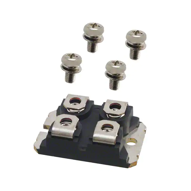
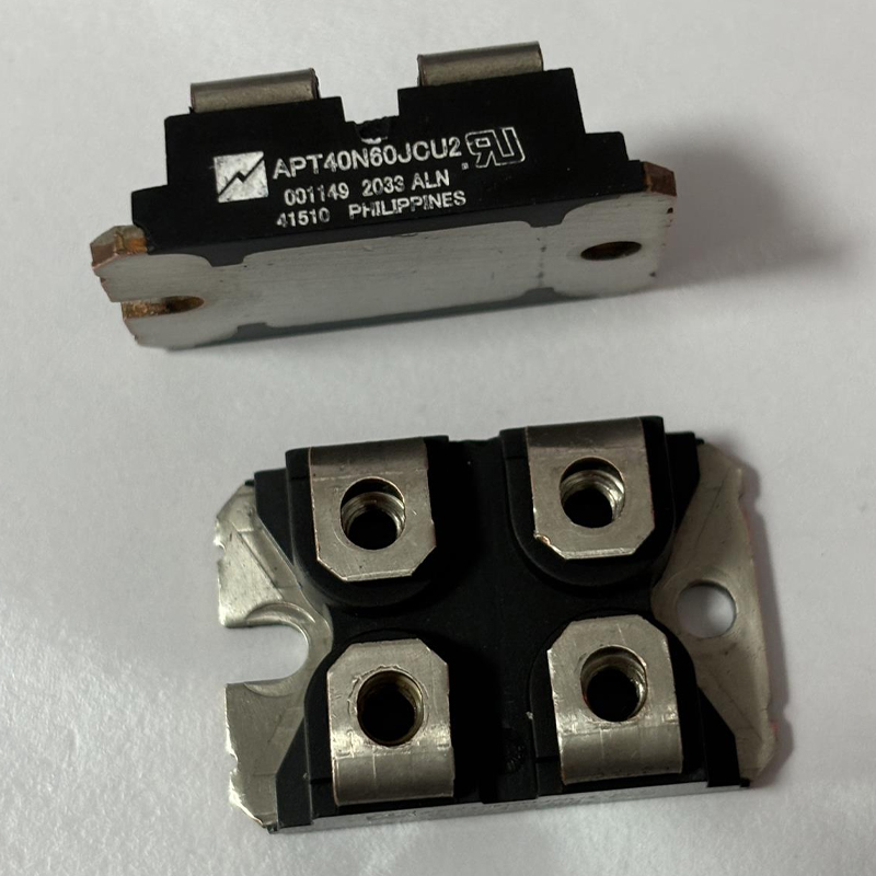
The APT40N60JCU2 SOT-227 MOSFET module uses the well-known ISOTOP power-module format.
This package is designed for significantly higher power levels than ordinary PCB-mounted transistor packages.
It allows the semiconductor module to be mechanically attached to a heat sink or cooling plate while providing an electrically isolated mounting structure.
For industrial systems, this can simplify thermal and mechanical integration.
The large base area supports practical thermal coupling to a suitable industrial heat sink.
The isolated module structure can simplify mounting compared with power devices whose metal mounting surface is electrically live.
Large power terminals are better suited to high-current wiring and bus structures than small PCB leads.
Mechanical mounting still matters. Heat-sink flatness, thermal interface material, screw torque and pressure distribution can all influence the final junction temperature.
Thermal Design for APT40N60JCU2
Thermal management is one of the most important parts of using APT40N60JCU2 successfully.
The device has a maximum junction temperature of 150°C. This represents an operating limit rather than a recommended continuous design target.
Designs intended for long industrial service normally benefit from maintaining meaningful temperature margin.
The maximum specified power dissipation can only be understood together with case temperature and thermal resistance.
Real heat must move from the silicon junction through the module, through the thermal interface, into the heat sink and finally into the surrounding environment.
- Calculate expected RMS MOSFET current.
- Correct RDS(on) for operating temperature.
- Estimate turn-on switching loss.
- Estimate turn-off switching loss.
- Include switching-frequency effects.
- Calculate worst-case junction temperature.
- Select suitable thermal-interface material.
- Choose an adequate heat sink.
- Evaluate airflow or forced cooling.
- Measure case temperature during prototype testing.
A large power module does not remove the need for thermal engineering. It simply provides a more practical path for moving heat out of the semiconductor.
Understanding the 600V Drain-Source Rating
APT40N60JCU2 belongs to the 600V MOSFET power module class.
This makes it suitable for many converter systems based on rectified AC mains or high-voltage DC buses.
However, designers should never assume that a 600 V MOSFET can safely operate with a normal repetitive drain voltage extremely close to 600 V.
Real switching circuits contain transformer leakage inductance, wiring inductance, package inductance, diode recovery effects and rapid current transitions.
These effects can create short voltage spikes above the steady-state DC-bus voltage.
A suitable voltage margin should therefore be included in the design. Snubber circuits, clamps, careful PCB layout and optimized switching speed can also help control drain-voltage overshoot.
APT40N60JCU2 for Power Factor Correction
Power factor correction is one of the most natural applications for a 600V Super Junction MOSFET.
A typical boost PFC circuit receives rectified AC mains and controls current through an inductor.
The objective is to shape the input current while producing a regulated high-voltage DC bus.
The MOSFET may switch tens of thousands of times every second while blocking hundreds of volts.
This operating environment rewards a device with suitable voltage margin, low conduction resistance and controlled switching performance.
APT40N60JCU2 combines Super Junction technology with a boost-chopper module configuration, making PFC one of its most important practical design areas.
Engineers should still optimize the gate resistor, boost diode, inductor, DC-link capacitor, current loop and thermal design together rather than treating the MOSFET as an independent component.
APT40N60JCU2 in Motor Control
Motor-control electronics contain rapidly changing current and significant stored magnetic energy.
Depending on the system architecture, a high-voltage power MOSFET module can be used in auxiliary converters, braking stages, DC-link circuits and other high-power switching functions.
When APT40N60JCU2 is considered for a motor-control system, engineers should evaluate maximum bus voltage, peak current, regenerative braking, switching frequency, cooling and fault conditions.
Motor loads are highly dynamic. A design that operates well during steady speed may experience very different current and voltage conditions during acceleration, deceleration or sudden braking.
For that reason, system-level testing should include realistic motor load profiles rather than only a static electronic load.
APT40N60JCU2 in Switched-Mode Power Supplies
The APT40N60JCU2 power MOSFET module can also be relevant to high-power switched-mode power supplies.
Potential systems include industrial power converters, telecom power systems, charging equipment, welding electronics, UPS systems, laboratory power supplies and specialized DC/DC converters.
Different converter topologies place very different stress on a MOSFET.
A hard-switched boost converter may emphasize turn-on loss and diode recovery. A resonant converter may reduce switching overlap but impose other current and timing requirements.
Therefore, engineers should evaluate the device using the actual topology rather than relying only on the words "600V" and "40A."
APT40N60JCU2 for Brake Switch Applications
The original application guidance for this device family also includes brake switching.
In an industrial motor drive, a decelerating motor may return energy to the DC bus.
If the system cannot send that energy back to the power grid or store it elsewhere, the DC-link voltage can rise.
A brake chopper can connect a resistor to the DC bus and convert the regenerative energy into heat.
The MOSFET in this circuit may need to block high bus voltage while conducting intense current pulses during braking events.
Peak pulse current, pulse duration, repetition rate, heat-sink capacity, braking resistor value and maximum bus voltage all need to be considered during design.
PCB, Busbar and Wiring Design Around APT40N60JCU2
The SOT-227 package is designed for high-power hardware, but poor external layout can still reduce its electrical performance.
Every high-current conductor contains some parasitic inductance. When current changes rapidly, that inductance creates voltage.
For this reason, switching-current loops around APT40N60JCU2 should be kept short and wide.
The DC-link capacitor should be positioned so the high-frequency current loop is as compact as practical.
Snubber components should also be connected close to the devices they are intended to protect.
The gate-driver circuit deserves separate attention. The gate and source path should remain compact and should not share unnecessary inductance with the main power-current path.
In high-power electronics, physical layout is part of the electrical circuit. A few centimeters of conductor can influence switching waveforms, overshoot and EMI.
Can APT40N60JCU2 Modules Be Connected in Parallel?
Power MOSFET modules can sometimes be connected in parallel when one device does not provide enough current capability.
MOSFET on-state resistance generally increases with temperature in the useful operating region. This behavior can help support static current sharing.
However, successful paralleling requires more than this positive temperature coefficient.
Each module should see similar drain resistance, source inductance, gate resistance and thermal conditions.
Different gate-loop inductance can cause one device to turn on faster than another and temporarily carry much more switching current.
For high-power designs, both static current sharing and dynamic switching current should be measured during prototype testing.
APT40N60JCU2 Replacement and Equivalent Selection
Searches for APT40N60JCU2 replacement and APT40N60JCU2 equivalent are especially important for engineers maintaining established industrial equipment.
A substitute should never be selected only because it is also described as a 600 V 40 A MOSFET.
Power-device replacement requires both static and dynamic comparison.
| Replacement Check | APT40N60JCU2 Reference | Why It Matters |
|---|---|---|
| Voltage Rating | 600 V | Must tolerate DC bus and switching transients |
| Current Rating | 40 A at Tc = 25°C | Changes current and thermal capability |
| RDS(on) | 70 mΩ max | Directly influences conduction loss |
| Technology | Super Junction MOSFET | Influences switching characteristics |
| Package | SOT-227 / ISOTOP | Must fit the original mechanical assembly |
| Internal Configuration | Boost Chopper | Electrical connections must match the circuit |
| Gate Charge | 259 nC typical | Can change gate-driver requirements |
| Switching Characteristics | Compare datasheet values and curves | Changes switching loss, ringing and EMI |
| Thermal Performance | Check junction-to-case data | Changes required cooling capacity |
| Mechanical Interface | SOT-227 mounting format | Affects heat sink and terminal compatibility |
A modern Super Junction MOSFET may provide lower switching loss or lower RDS(on), but it may also switch faster than the original device.
That can increase ringing or EMI if the original gate driver and layout were designed around slower switching behavior.
For this reason, a replacement should be validated in the actual power converter before production use.
APT40N60JCU2 vs Modern SiC MOSFET Modules
Silicon carbide technology has become increasingly common in high-power conversion.
SiC MOSFETs can offer fast switching, high breakdown voltage and strong high-temperature operation.
This naturally makes SiC devices potential candidates when engineers search for an APT40N60JCU2 replacement.
However, replacing a silicon Super Junction MOSFET with SiC is not automatically a drop-in upgrade.
A faster SiC switch can increase dv/dt and di/dt. That may expose weaknesses in gate-drive circuits, insulation systems, snubber networks, PCB layout and EMI filters.
The replacement must also match mechanical mounting, terminal layout, voltage rating, current rating and cooling requirements.
For a completely new platform, SiC may provide major efficiency and power-density benefits. For an existing industrial repair, a closely matched silicon replacement may sometimes require much less engineering change.
APT40N60JCU2 Lifecycle and Legacy Design Considerations
Lifecycle information is important when dealing with older power semiconductor modules.
Distribution channels may classify APT40N60JCU2 as an older or obsolete component, so engineers planning a new long-term production design should verify current manufacturer and distributor status before finalizing the BOM.
Existing industrial equipment may still require the original module for repair, maintenance or legacy production.
This creates continuing demand for searches such as APT40N60JCU2 in stock, APT40N60JCU2 replacement and APT40N60JCU2 equivalent.
For new projects, it may be sensible to qualify an alternative component early rather than waiting until remaining inventory becomes difficult to source.
How to Buy APT40N60JCU2 Safely
People searching buy APT40N60JCU2, APT40N60JCU2 price or APT40N60JCU2 in stock are often supporting high-value industrial equipment.
For a power module, component quality matters because a semiconductor failure can affect gate drivers, DC-link capacitors, fuses, control electronics and connected machinery.
- Confirm the complete APT40N60JCU2 part number.
- Verify the SOT-227 / ISOTOP package.
- Check manufacturer markings.
- Confirm the boost-chopper configuration.
- Request traceability when required.
- Inspect terminals and package condition.
- Review date-code requirements.
- Check storage conditions for older stock.
- Confirm the required production quantity.
- Evaluate long-term replacement options.
For production purchasing, price should be considered together with authenticity, traceability, availability and long-term supply risk.
A cheaper power semiconductor is not necessarily a lower-cost purchase if quality or traceability problems create failures in expensive industrial equipment.
How to Read the APT40N60JCU2 Datasheet
An APT40N60JCU2 datasheet should be used as more than a list of maximum ratings.
Engineers should review the electrical-characteristic tables together with the performance graphs.
Useful areas include RDS(on) versus temperature, gate-charge behavior, capacitance curves, switching energy, safe operating area, thermal resistance and package dimensions.
Graphs are particularly important because MOSFET behavior changes continuously with current, voltage and junction temperature.
For example, an RDS(on) value specified around room temperature does not represent the same resistance when the junction is operating at a much higher temperature.
Likewise, switching-time measurements obtained with one gate resistor and one current level cannot describe every possible converter.
The datasheet should therefore be used as the starting point for engineering calculations, followed by measurements in the real application.
Common APT40N60JCU2 Applications
APT40N60JCU2 is designed for high-power switching rather than low-power signal control.
- Power factor correction systems
- Boost converter stages
- Industrial switched-mode power supplies
- AC motor-control equipment
- DC motor-control equipment
- Brake chopper circuits
- Industrial power conversion
- High-voltage DC systems
- Welding power equipment
- UPS power stages
- Battery charging systems
- Industrial automation power supplies
The device is most valuable when its 600 V voltage capability, Super Junction MOSFET structure, boost-chopper topology and heat-sink-mounted package match the electrical and mechanical requirements of the complete system.
Frequently Asked Questions About APT40N60JCU2
What is APT40N60JCU2?
APT40N60JCU2 is a 600 V N-channel Super Junction MOSFET power module with a boost-chopper configuration and SOT-227 / ISOTOP package.
What is the current rating of APT40N60JCU2?
The continuous drain-current rating is 40 A with the case at 25°C under the specified datasheet conditions. Current capability must be derated as operating temperature increases.
What is the voltage rating of APT40N60JCU2?
APT40N60JCU2 has a drain-source voltage rating of 600 V.
What is the APT40N60JCU2 RDS(on)?
The datasheet specifies a maximum drain-source on-resistance of approximately 70 mΩ under the stated test conditions.
What package does APT40N60JCU2 use?
APT40N60JCU2 uses an isolated SOT-227 / ISOTOP power-module package designed for heat-sink mounting.
Is APT40N60JCU2 a Super Junction MOSFET?
Yes. It uses N-channel Super Junction MOSFET technology intended for efficient high-voltage switching.
What is APT40N60JCU2 used for?
Typical application areas include power factor correction, switched-mode power supplies, motor-control electronics, boost converters and brake-switch circuits.
Can APT40N60JCU2 be replaced with another 600V 40A MOSFET?
Not automatically. A replacement should also be checked for RDS(on), gate charge, switching behavior, package, terminal layout, boost-chopper configuration, thermal resistance and mechanical compatibility.
Is APT40N60JCU2 suitable for PFC circuits?
Yes. Its 600 V Super Junction MOSFET technology and boost-chopper configuration make power factor correction one of its important application areas.
Where can I buy APT40N60JCU2?
Availability can vary because it is an older power-semiconductor module. Buyers should verify exact part numbers, stock condition, traceability and supplier quality before purchasing.
Final Thoughts on APT40N60JCU2
The APT40N60JCU2 is best understood as an integrated high-power switching solution rather than simply a generic 600V 40A MOSFET.
Its combination of 600 V drain-source capability, 40 A current rating, 70 mΩ maximum on-resistance, Super Junction technology and isolated SOT-227 / ISOTOP construction makes it suitable for demanding high-voltage power-conversion applications.
The boost-chopper configuration is especially relevant to power factor correction and related converter stages, while the large module format supports practical heat-sink mounting in industrial equipment.
Gate charge and switching performance are just as important as on-state resistance. A suitable gate driver must control the device quickly enough to limit switching loss without generating unnecessary ringing or electromagnetic interference.
The strongest APT40N60JCU2 design considers voltage margin, current waveform, RDS(on), switching energy, gate drive, thermal resistance, stray inductance and mechanical mounting as one complete system.
Thermal design is equally important. The headline current and power ratings assume defined case-temperature conditions, so real current capability depends heavily on heat-sink design and the complete junction-to-ambient thermal path.
For legacy equipment, replacement selection deserves particular care. Two devices can share the same nominal voltage and current ratings while having very different gate charge, switching speed, thermal performance or internal configuration.
For new production designs, component lifecycle should also be considered. If long-term availability is uncertain, qualifying a technically suitable alternative early can reduce future supply-chain risk.
Whether the goal is PFC, motor control, switched-mode power conversion, braking or industrial equipment repair, understanding the complete electrical and thermal behavior of APT40N60JCU2 is more useful than treating it as only another high-voltage MOSFET.