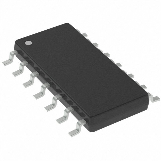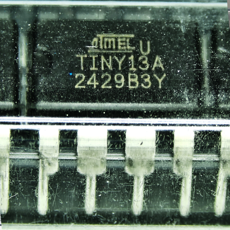
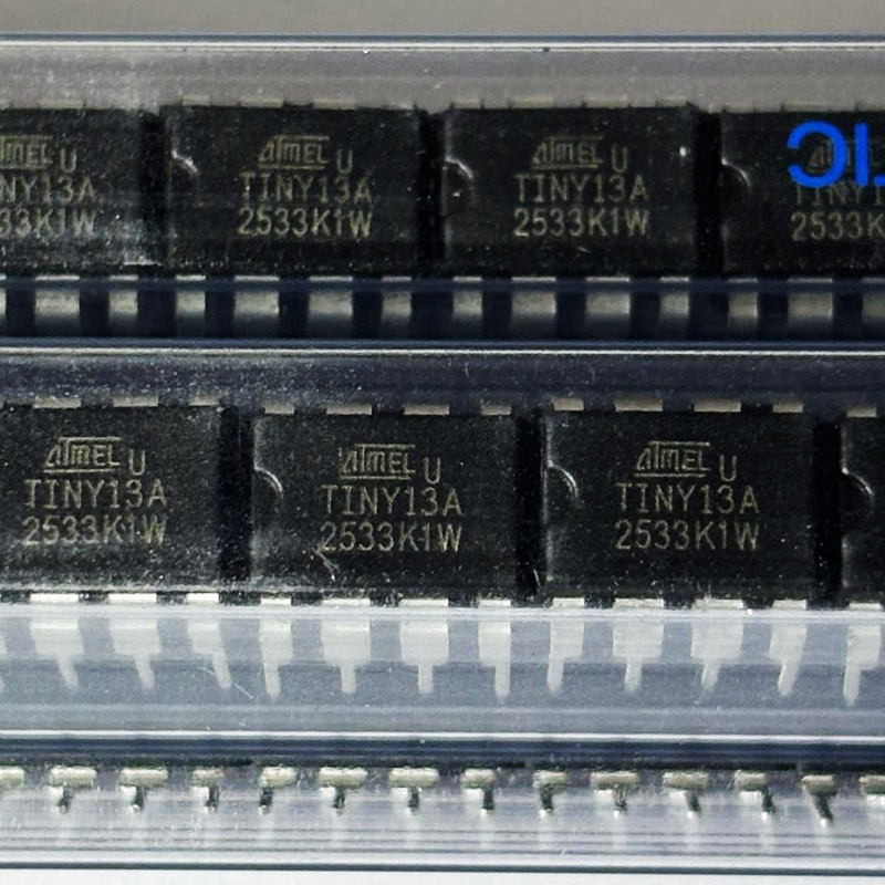
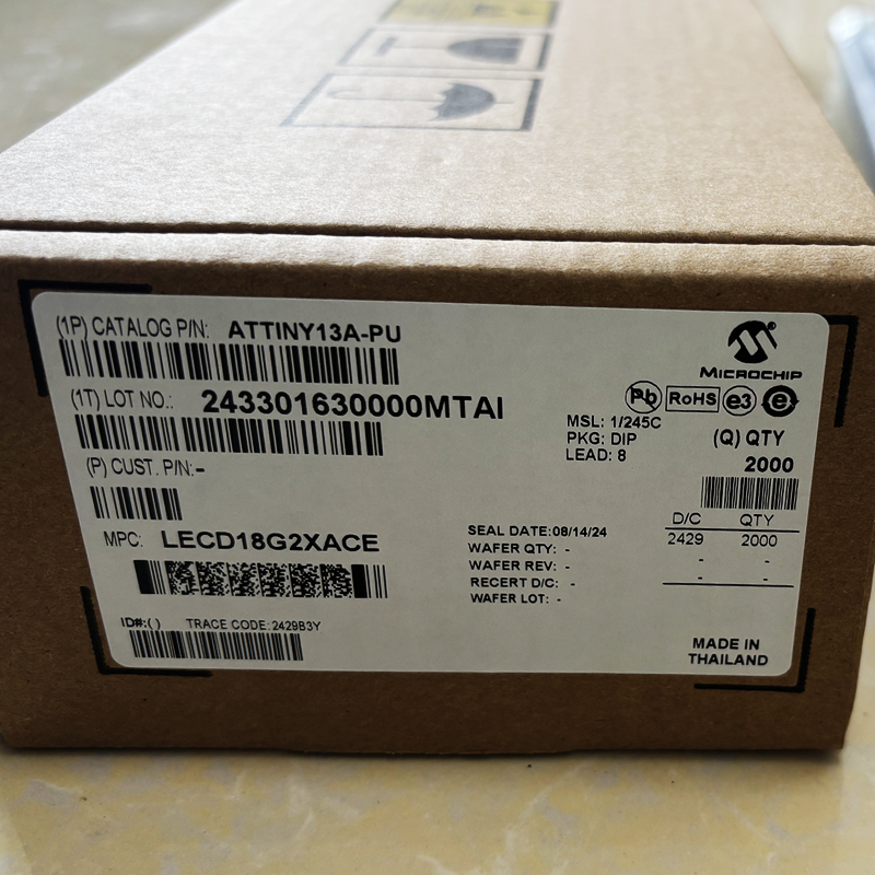
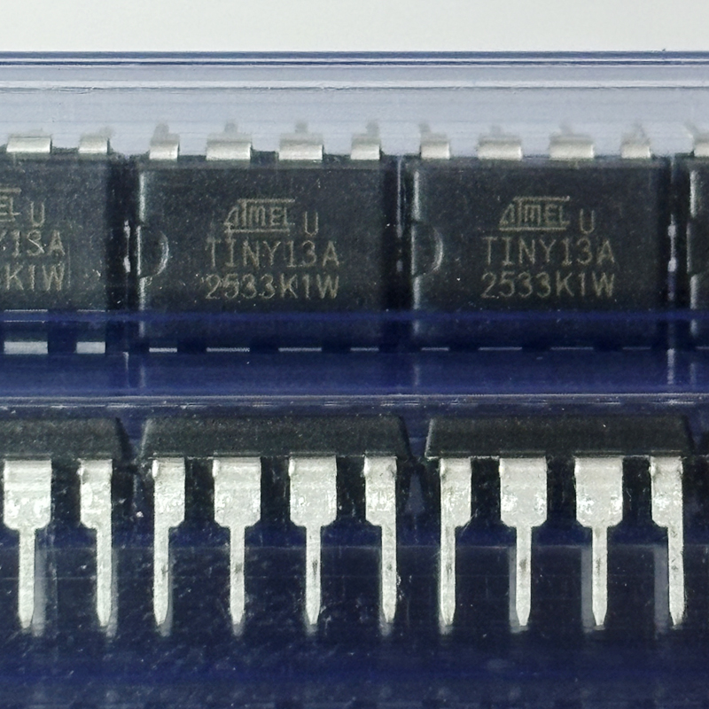


ATTINY13A-PU 8-Bit AVR Microcontroller: Specifications, Pinout, Applications, and Design Guide
The ATTINY13A-PU is a compact 8-bit AVR microcontroller for focused embedded-control tasks. Its 1KB Flash, 64-byte SRAM, 64-byte EEPROM, 10-bit ADC, timer, PWM, watchdog, and easy-to-handle PDIP-8 package make it useful for sensors, LED control, timing, compact automation, prototypes, and dedicated electronic functions.
What is ATTINY13A-PU? ATTINY13A-PU is an 8-bit AVR microcontroller from Microchip with 1KB of programmable Flash, 64 bytes of SRAM, 64 bytes of EEPROM, six programmable I/O lines, a four-channel 10-bit ADC, an 8-bit Timer/Counter, two PWM channels, watchdog functions, and SPI in-system programming. The PU ordering option uses an 8-pin PDIP through-hole package.
Not every electronic design needs a large processor. Many products repeatedly perform only a few actions: read a switch, measure a sensor voltage, compare a value with a threshold, generate PWM, control an indicator, supervise a battery, or activate an external driver. For these jobs, a small microcontroller can create a cleaner design than a device with unused memory and peripherals.
The ATTINY13A-PU should therefore be judged by fit rather than size. Its limited resources demand careful firmware, but they also encourage direct architecture, predictable behavior, low component count, and clear ownership of each pin and byte.
What Makes the ATTINY13A-PU Different?
The ATtiny13A is a low-power CMOS microcontroller based on the AVR enhanced RISC architecture. Many instructions execute in one clock cycle, allowing the device to provide useful control performance without a large software platform. It includes 32 general-purpose working registers and can approach one MIPS per megahertz under suitable conditions.
The ATTINY13A-PU PDIP-8 version is especially practical for breadboards, sockets, repairable prototypes, test fixtures, education, laboratories, and low-volume production. Through-hole packaging occupies more board space than a surface-mount option, but it is easier to insert, remove, inspect, and solder manually.
A 1KB program limit is a real constraint, but it can also improve design discipline. It pushes the developer to remove unnecessary libraries, avoid oversized abstractions, and define the product's actual control task before writing firmware.
ATTINY13A-PU Complete Specification Table
The following table summarizes the device resources that matter most during part selection. Electrical limits and alternate pin functions should still be verified against the current datasheet for the exact ordering code.
| Specification | ATTINY13A-PU Value | Design Meaning |
|---|---|---|
| CPU Architecture | 8-bit AVR enhanced RISC | Designed for compact, deterministic embedded control. |
| Maximum Clock | Up to 20 MHz | Maximum frequency requires the supported voltage range. |
| Flash Memory | 1KB | Stores executable firmware; code-size planning is essential. |
| SRAM | 64 bytes | Shared by variables, temporary data, buffers, and stack. |
| EEPROM | 64 bytes | Stores small settings and calibration values after power loss. |
| Programmable I/O | Six lines | Pins are multiplexed with ADC, PWM, reset, clock, and programming functions. |
| ADC | Four-channel, 10-bit | Measures suitable analog sensor and voltage signals. |
| Timer | One 8-bit Timer/Counter | Supports timing, counting, compare functions, and PWM. |
| PWM | Two channels | Useful for LED dimming, pulse generation, and external driver control. |
| Programming | In-system programming through SPI | Firmware can be loaded after the MCU is assembled on the PCB. |
| Supply Voltage | 1.8V to 5.5V | Frequency must be selected according to the voltage speed grade. |
| Package | 8-lead PDIP, package code 8P3 | Convenient for breadboards, sockets, manual assembly, and service. |
| Temperature Range | −40°C to +85°C for ATTINY13A-PU | System-level environmental qualification is still required. |
ATTINY13A-PU PDIP-8 Pinout and Pin Functions
Every pin matters on an 8-pin controller. Several pins combine general-purpose I/O with ADC, PWM, serial programming, comparator, interrupt, reset, or clock functions. Pin allocation should therefore be completed before the firmware architecture is fixed.
Disabling the RESET function to reclaim PB5 as ordinary I/O can complicate future programming and recovery. Make fuse changes only when the programming method and recovery path are fully understood.
Understanding the 1KB Flash, 64B SRAM, and 64B EEPROM
The three memory types serve different jobs. Flash holds the executable program, SRAM holds temporary runtime data, and EEPROM stores selected information that should remain after power is removed. Treating them as separate budgets prevents late-stage firmware problems.
1KB Flash Program Memory
Flash stores the compiled application. One kilobyte is enough for a focused state machine, sensor threshold controller, LED pattern, simple timing function, PWM controller, or monitoring task. Large frameworks and general-purpose libraries can consume the space quickly, so compile representative functions early.
64 Bytes of SRAM
SRAM is shared by variables, temporary values, buffers, local data, and the stack. A small source file can still use too much SRAM if it includes arrays, formatted strings, deep function calls, or unnecessary copies. Process data as it arrives and reuse storage where the behavior remains clear.
64 Bytes of EEPROM
EEPROM is useful for calibration values, selected modes, counters, thresholds, or other small parameters that must survive power loss. Because EEPROM has finite write endurance, firmware should avoid writing unchanged values or updating the same location unnecessarily.
Clock Speed and Supply Voltage Must Be Selected Together
The ATTINY13A-PU supports a broad 1.8V to 5.5V supply range, but the maximum permitted clock rate changes with voltage. The official speed grades are 0–4 MHz at 1.8–5.5V, 0–10 MHz at 2.7–5.5V, and 0–20 MHz at 4.5–5.5V.
| Supply Condition | Supported Clock Range | Practical Design Note |
|---|---|---|
| 1.8V to 5.5V | 0 to 4 MHz | Useful for lower-voltage and energy-conscious control systems. |
| 2.7V to 5.5V | 0 to 10 MHz | Balances processing speed with common 3.3V and 5V supplies. |
| 4.5V to 5.5V | 0 to 20 MHz | Required for operation at the device's maximum rated clock. |
The calibrated internal oscillator can reduce external component count when the application does not need a specialized clock source. Designers should still evaluate oscillator tolerance, temperature, supply variation, timing accuracy, and fuse settings against the real application.
Using the Four-Channel 10-Bit ADC
The integrated ADC converts a suitable analog voltage into a digital value that firmware can process. This makes ATTINY13A-PU useful for potentiometers, conditioned temperature sensors, light-sensing circuits, battery-divider measurements, current-monitor front ends, and other low-complexity analog inputs.
A 10-bit result provides 1024 nominal code levels. Actual measurement quality depends on reference stability, source impedance, grounding, decoupling, switching noise, PCB layout, sampling strategy, and calibration. The number of bits in the specification does not guarantee the same number of noise-free bits in a finished product.
Does ATTINY13A-PU have an ADC? Yes. It includes a four-channel, 10-bit ADC with an internal voltage reference. The ADC inputs share package pins with other digital and alternate functions.
Timer, PWM, Interrupt, and Watchdog Functions
The device includes one 8-bit Timer/Counter with a prescaler and two PWM channels. Hardware timing can manage periodic sampling, pulse generation, event counting, compare matches, repeated output changes, LED brightness, or control signals for an external power stage.
PWM pins must not directly drive loads beyond the MCU's electrical ratings. Motors, relays, solenoids, heaters, and high-power LEDs usually require a transistor, MOSFET, driver IC, flyback protection, current limiting, or isolation according to the load.
A programmable watchdog timer with a separate on-chip oscillator can help recover from certain software failures. It should be treated as one layer of reliability, not a substitute for correct state handling, input validation, power design, and fault testing.
Common ATTINY13A-PU Applications
The strongest applications are narrow, repeatable, and easy to define. ATTINY13A-PU often works best as a dedicated controller responsible for one local function rather than as the main processor of a complex product.
LED and Indicator Control
PWM and timer functions support dimming, flash patterns, warning indicators, and compact lighting behavior.
Sensor Threshold Monitoring
The ADC can measure a conditioned analog signal and compare it with firmware-defined operating limits.
Simple Motor or Power Control
PWM can command an external driver for basic speed or power-level control while keeping high current outside the MCU.
Battery-Powered Devices
Wide-voltage operation and sleep modes can support efficient designs when the entire circuit is optimized for low current.
Timing and Alarm Products
The Timer/Counter, interrupts, and watchdog support repeated timing events, alarms, delays, and recovery behavior.
Dedicated Companion Controller
A small MCU can supervise one local function while a larger processor manages communication, display, or application logic.
How to Program ATTINY13A-PU
The ATtiny13A supports in-system programming through its SPI programming interface. On the PDIP-8 device, the programming signals share PB0/MOSI, PB1/MISO, PB2/SCK, and PB5/RESET. VCC and GND are also required by the programming arrangement.
A production PCB should provide suitable pads or a connector before layout is complete. Good access reduces fixture complexity and makes firmware loading, testing, diagnosis, and servicing easier. The programming circuit must also account for any other components attached to shared pins.
Confirm device selection, supply voltage, programmer connection, clock configuration, reset behavior, fuse settings, and pin loading before changing configuration bits. Keep a documented recovery plan for fuse choices that affect RESET or clock operation.
Low-Power Design with ATTINY13A-PU
The controller provides Idle, ADC Noise Reduction, and Power-down modes. Real battery life, however, depends on more than the MCU mode. Sensors, regulator quiescent current, pull resistors, LEDs, external drivers, input states, wake frequency, and leakage paths may consume more energy than the controller.
A useful low-power strategy is to define how long the product sleeps, what event wakes it, which peripherals must remain active, how quickly it can finish its work, and when it returns to sleep. Measure the complete board over realistic operating cycles instead of relying only on a single datasheet current figure.
When Should You Choose ATTINY13A-PU?
- The firmware task is small, stable, and clearly defined.
- One timer, two PWM outputs, and four ADC channels cover the requirement.
- A breadboard-friendly or socketable PDIP-8 package adds value.
- Only a small amount of non-volatile configuration data is required.
- Low component count and direct control are important.
- The MCU performs one dedicated local function.
- The application approaches the 1KB Flash or 64-byte SRAM limit.
- Large buffers, strings, protocol stacks, or software frameworks are needed.
- The design requires more independent pins or communication peripherals.
- Future features are likely to expand significantly.
- Debugging, bootloading, or complex field-update requirements need more resources.
ATTINY13A-PU Design Checklist Before Production
- Verify the exact ordering codeConfirm the ATTINY13A-PU package, temperature range, marking, and approved sourcing documentation.
- Compile representative firmware earlyTrack Flash use while core features are developed instead of waiting until the PCB is complete.
- Measure SRAM useAccount for globals, locals, stack, interrupts, buffers, and temporary compiler-generated data.
- Plan every multiplexed pinResolve ADC, PWM, reset, clock, interrupts, digital I/O, and programming conflicts before layout.
- Match clock to voltageDo not operate at 20 MHz unless the supply and conditions satisfy the corresponding speed grade.
- Add local decouplingPlace an appropriate bypass capacitor close to the VCC and GND pins and design the complete power path carefully.
- Protect external interfacesUse suitable drivers, current limiting, flyback suppression, ESD protection, level conversion, or isolation as required.
- Validate ADC behavior on the final PCBTest noise, grounding, reference stability, source impedance, filtering, and calibration with real sensors.
- Keep programming accessProvide reliable access to SPI programming signals and document fuse settings and recovery procedures.
- Test abnormal conditionsVerify startup, brownout, watchdog recovery, unexpected inputs, supply variation, temperature, and load faults.
ATTINY13A-PU Frequently Asked Questions
These concise answers cover the questions most often asked during selection, purchasing, prototyping, and firmware planning.
What is ATTINY13A-PU?
It is an 8-bit AVR microcontroller with 1KB Flash, 64-byte SRAM, 64-byte EEPROM, ADC, timer, PWM, watchdog, analog comparator, interrupts, and SPI in-system programming in an 8-pin PDIP package.
How much Flash and RAM does ATTINY13A-PU have?
It provides 1KB of programmable Flash and 64 bytes of internal SRAM. Firmware size, variables, buffers, and stack use must be managed carefully.
Does ATTINY13A-PU have EEPROM?
Yes. It includes 64 bytes of EEPROM for small settings, calibration values, counters, modes, or other data that should survive power loss.
Does ATTINY13A-PU have an ADC?
Yes. It includes a four-channel, 10-bit ADC with an internal voltage reference. The analog channels share pins with other functions.
Does ATTINY13A-PU support PWM?
Yes. Its 8-bit Timer/Counter provides two PWM channels, OC0A and OC0B, available through shared package pins.
What is the maximum ATTINY13A-PU clock speed?
The device supports up to 20 MHz at 4.5V to 5.5V. Lower supply voltages have lower maximum clock ranges.
What voltage does ATTINY13A-PU use?
Its operating supply range is 1.8V to 5.5V. The selected clock frequency must comply with the voltage-dependent speed grade.
How is ATTINY13A-PU programmed?
It supports in-system programming through SPI using MOSI, MISO, SCK, RESET, VCC, and GND connections.
What package does ATTINY13A-PU use?
The PU option uses an 8-lead PDIP through-hole package, identified as package code 8P3 in the ordering information.
Is ATTINY13A-PU suitable for beginners?
The PDIP-8 package is convenient for breadboards and manual experiments. Its small memory also teaches careful firmware, pin planning, fuse management, and direct use of hardware peripherals.
What is ATTINY13A-PU commonly used for?
Common uses include LED control, sensor monitoring, timing circuits, small alarms, PWM output, battery electronics, compact automation, educational projects, and dedicated companion-control functions.
When should I use a larger microcontroller?
Use a larger MCU when the project needs more program memory, RAM, pins, communication interfaces, buffers, complex libraries, advanced debugging, or substantial future expansion.
Final View: Why ATTINY13A-PU Still Fits Small Embedded Designs
The ATTINY13A-PU is valuable when the application needs a small amount of programmable intelligence rather than a general-purpose computing platform. Its ADC, timer, PWM, interrupts, watchdog, EEPROM, and flexible I/O can replace several discrete control functions while keeping the board understandable.
The PDIP-8 package also remains useful for breadboards, sockets, education, repair, laboratory work, and low-volume production. The device can be inserted, removed, and replaced without fine-pitch assembly equipment.
The central design rule is simple: respect the limits. Plan Flash, SRAM, pins, clock, voltage, programming access, and external loads before the project expands. When the requirement fits, ATTINY13A-PU provides a direct and practical controller. When it does not fit, selecting a larger MCU early is better than forcing an oversized feature set into a very small device.