Engineering-Driven PCBA Custom Services
We don't just assemble; we optimize. Send us your Gerber files and BOM for a comprehensive DFM review, cost reduction analysis, and IPC-standard manufacturing.
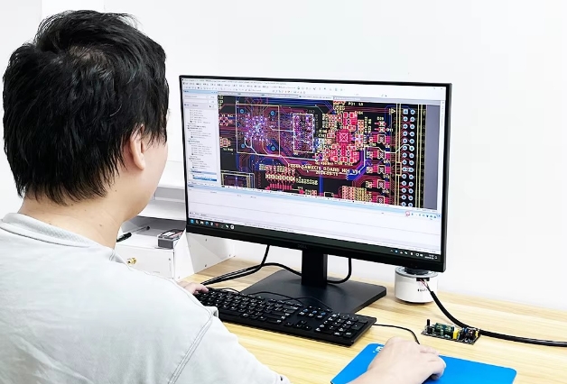 DFM service
DFM Review & Optimization
Identify potential manufacturing issues before production begins to ensure high yield rates and stable quality.
- Design for Manufacturability (DFM)
- Gerber optimization
- Direct engineer-to-engineer support
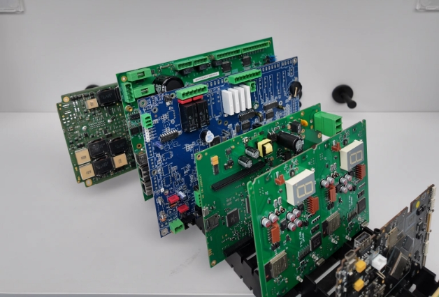 PCBA Service
BOM Optimization & Sourcing
Reduce hidden costs and stabilize your supply chain with our professional component sourcing and alternative recommendations.
- Transparent pricing structure
- Reliable component alternatives
- Authorized dealer procurement
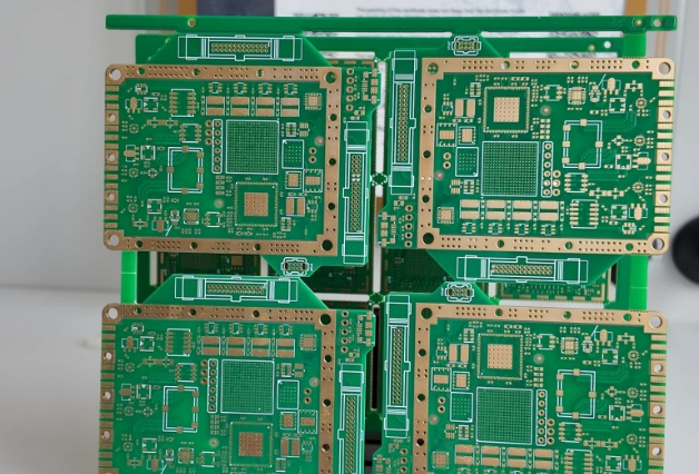 PCB Manufacturing
Precision PCB Panelization Optimization
Optimized panel layout maximizes board output, reduces material waste, and significantly lowers unit cost per PCB.
- IPC-A-610 standard execution
- AOI / SPI automated inspection
- ISO9001 & ISO14001 certified
 Partnership-Support NDA
DFM Review & Optimization
Identify potential manufacturing issues before production begins to ensure high yield rates and stable quality.
- Design for Manufacturability (DFM)
- Gerber optimization
- Direct engineer-to-engineer support
If you have already sent the Gerber files, please wait for our engineering team to review.
GLOBAL ENGINEERING SUPPORT
Select your region for localized PCBA manufacturing services and technical communication.
Common PCBA Outsourcing Bottlenecks
Are these critical issues disrupting your electronic manufacturing supply chain? If you've worked with PCBA suppliers before, you've likely faced these issues. We understand the engineering and operational hurdles you face.


Opaque Pricing & Hidden Fees
Unexpected costs, unclear BOM pricing, and sudden surcharges that destroy your project budget and profit margins.
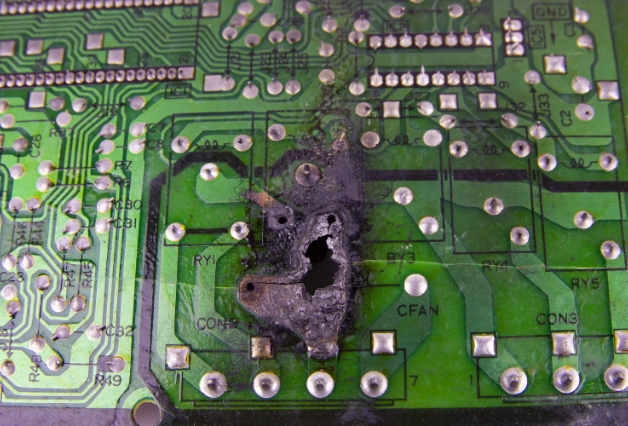

Unstable Quality & Rework
Inconsistent batch quality, high failure rates,rework, reliability concerns and lack of IPC standard compliance leading to costly field failures.


Unreliable Delivery Schedules
Missed deadlines, unreliable lead time delays, supply chain disruptions, and poor production planning that severely delay your time-to-market.


Inefficient Communication
Language barriers, slow response times, and lack of direct access to experienced engineers when technical issues arise.
How We Solve PCBA Manufacturing Challenges
We are more than just a PCBA manufacturer-we are solution creators. We implement a dedicated project team for each order, including a sales representative, engineer, supply chain specialist, and quality manager. They are fully involved throughout your project, conducting rigorous reviews of your Gerber files and BOM to eliminate hidden costs, prevent rework, ensure on-time delivery, and maintain seamless communication.
 01
01
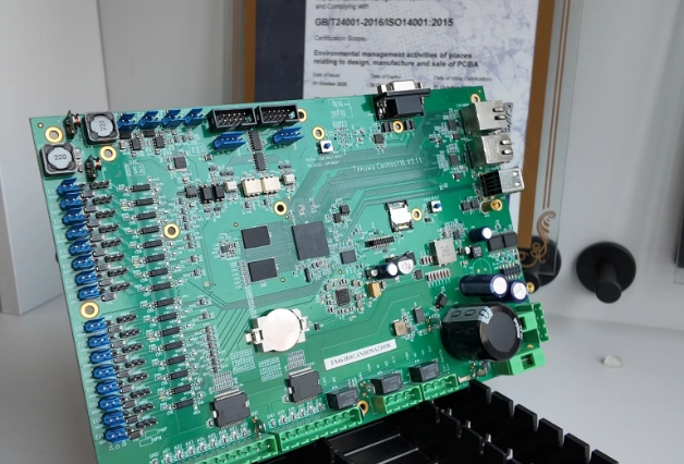
BOM Optimization
Strategic analysis of your Bill of Materials to identify cost-reduction opportunities. We eliminate hidden fees and optimize component selection without compromising IPC standards.
 02
02
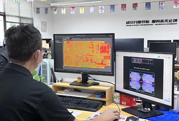
DFM Review
Comprehensive Design for Manufacturability (DFM) analysis on your Gerber files to identify potential risks, ensuring higher yield rates and preventing costly rework before production begins.
 03
03
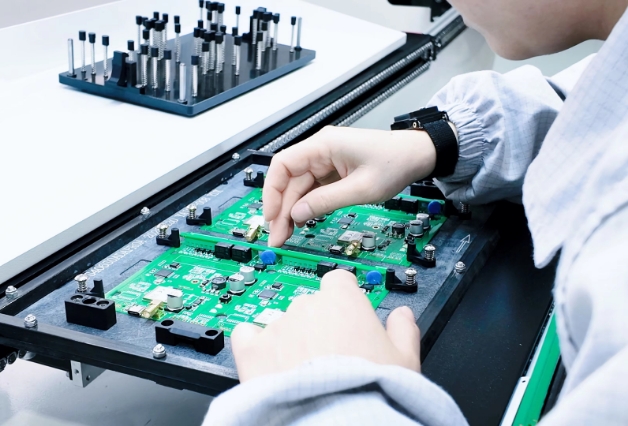
Component Substitution
Replace high-cost or unstable components with proactive sourcing of reliable high-quality alternative components to mitigate supply chain disruptions, ensuring your project stays on schedule with reliable delivery times.
 04
04
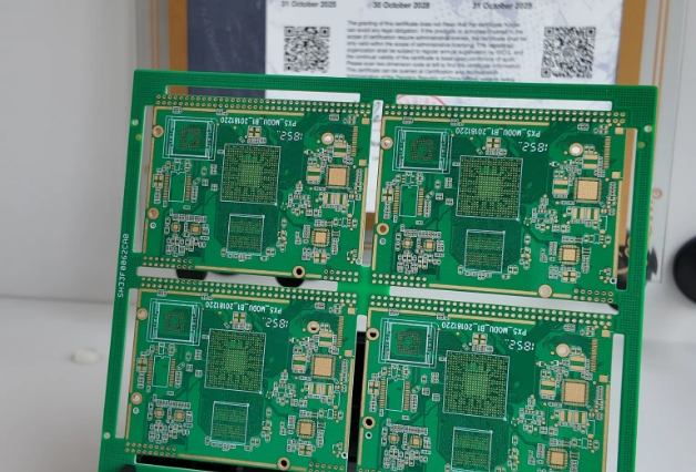
Panelization Optimization
Smart PCB array configurations designed by our engineers to maximize material usage, streamline the SMT assembly process, and significantly lower your overall unit price.
Ready to optimize your PCBA project?
Upload your Gerber files and BOM. Our engineering team will provide a comprehensive manufacturability review and an optimized quote.
How We Make It Happen
Executing precision and reliability through stringent standards, advanced facilities, and expert engineering support.
 01
01

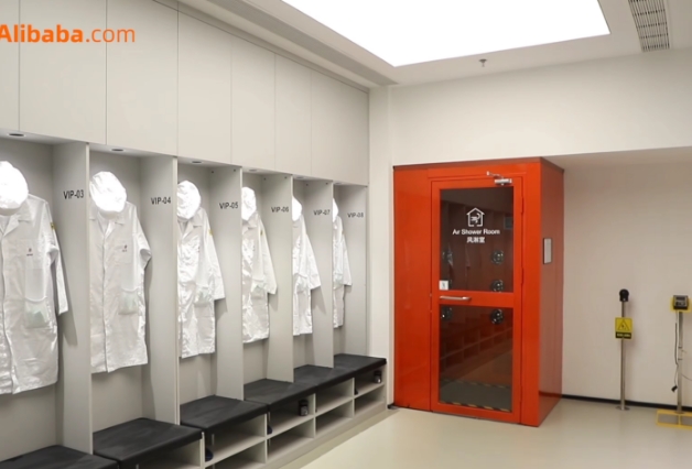
Strict ESD and air shower management.
Unlike many factories that treat ESD as an add-on, FC Electronic implements a strict and comprehensive Electrostatic Discharge control system.
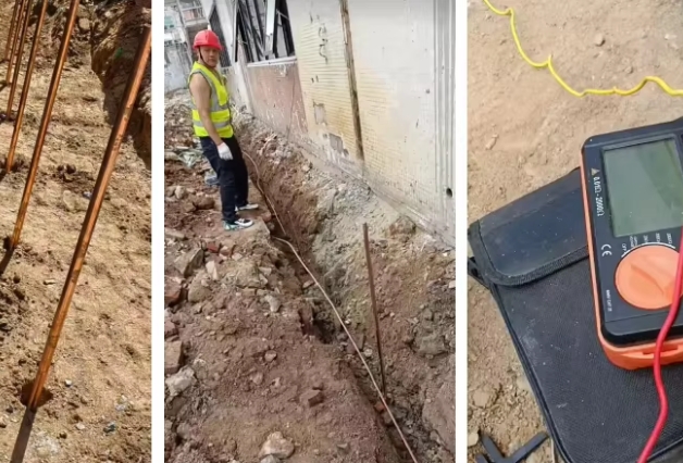

High-standard grounding resistance system.
Our facility is built with a stable, plant-wide grounding system that exceeds standard ESD requirements. While the typical grounding resistance standard is ≤4Ω, we achieve 0.98Ω-meeting the demands of high-reliability products.
 03
03

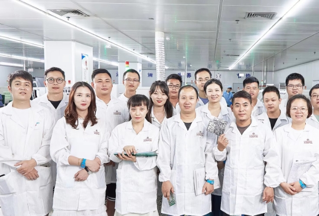
Direct Engineer Communication
Eliminate communication barriers. Our experienced R&D engineers work directly with your team for PCB DFM reviews and technical troubleshooting.
 04
04

Stable Supply Chain
Once you work with us, we immediately form a dedicated team-sales, project, BOM and NPI engineers, PMC, QC, and sourcing-leveraging Shenzhen's strong component supply and authorized networks to ensure reliable delivery and authenticity.
Advanced Manufacturing Capabilities
Precision PCBA production driven by state-of-the-art automation, rigorous IPC-A-610 standards, and comprehensive quality control for engineers and R&D teams.
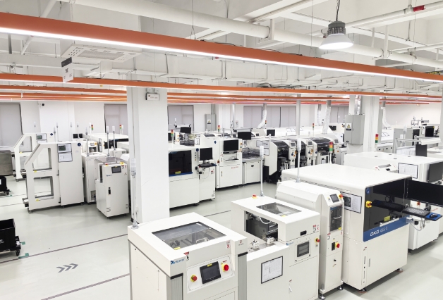 SMT Workshop
SMT Workshop
Our SMT lines are built for stable, high-precision production with full-process control from the start. FAT first article verification ensures every setup is validated before mass production, reducing early-stage defects and rework. An intelligent solder paste management system controls the entire lifecycle - from storage to usage and disposal - ensuring full traceability and consistent performance, far beyond basic storage used by most factories. With advanced solder paste printing and 3D SPI inspection with CCD verification, we ensure accurate deposition and minimize printing defects. A dedicated stencil room with inspection and cleaning systems further guarantees precision and repeatability. Ion cleaning removes invisible contamination before placement, improving soldering reliability. Our vertical buffer system stabilizes mixed production lines, reducing manual handling and enhancing efficiency. AI-powered 3D AOI analyzes solder joint height, volume and coplanarity, adapting to different products and batches while reducing false calls and improving inspection efficiency.
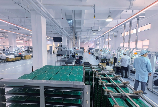 DIP Workshop
DIP Workshop
Advanced DIP Assembly for Reliable Through-Hole Performance Our DIP workshop is equipped with advanced technologies to ensure stable and high-quality through-hole assembly. Pre-wave soldering AOI machine inspection helps detect potential defects in advance, reducing rework and improving first-pass yield. We utilize precise wave soldering processes for efficient and consistent soldering performance. For complex and high-reliability applications, our rare-in-industry selective wave soldering machine enables targeted soldering, making it ideal for automotive, industrial, and medical PCBA projects. Our dedicated cleaning area ensures optimal board cleanliness based on component sensitivity. We combine machine cleaning, dry ice cleaning technology, and manual cleaning with mild solvents to protect sensitive components while ensuring long-term reliability.
Strategic Global Partnership
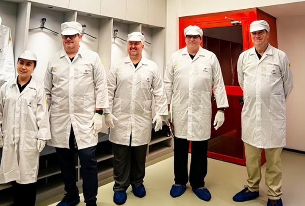
We don't just manufacture; we partner. Our leadership team conducts annual global visits to align with our clients' long-term technology roadmaps and resolve complex DFM challenges.
IPC-A-610 Class 2/3
Strict adherence to electronic assembly acceptability standards.
100% AOI & SPI Inspection
Automated optical inspection for every PCBA board produced.
ESD Controlled Environment
Full anti-static protection throughout the manufacturing process.
Remote Factory Experience
Verify our PCBA capabilities, ESD controls, and IPC-A-610 compliance from anywhere in the world. Transparent, real-time access to our manufacturing floor.

3D VR Factory Tour
Take a comprehensive virtual walk through our SMT lines, DIP processes, and QA testing facilities at your own pace. Inspect our equipment layout and cleanliness standards.
Start VR Tour
Live Video Audit
Schedule a live video conference with our production managers. Direct the camera to inspect specific AOI/SPI equipment, ESD controls, and standardized operations.
Book an Audit
Video Meeting
Hold real-time technical discussions with our engineers via video conference to review project details, address challenges, and resolve engineering issues directly.
Contact EngineeringWhy Choose Flychip
Engineering-driven PCBA manufacturing with uncompromising quality control and transparent processes.
PCBA Cleaning Process
Impacts long-term reliability and corrosion resistance
Quality Standards
Ensures consistent manufacturing excellence
Engineering Support
Technical assistance during pre-production
Factory Transparency
Verification of manufacturing capabilities
New Arrivals


HOW TO START YOUR PROJECT
Streamlined PCBA Customization & Engineering Process
Upload Gerber & BOM
Submit your complete manufacturing data securely. We require standard Gerber files and a detailed Bill of Materials for an accurate engineering assessment.
Engineering Evaluation
Our engineers conduct a thorough DFM review and BOM optimization to ensure manufacturability, component availability, and cost-efficiency.
Start Production
Upon approval, we initiate manufacturing under strict IPC-A-610 standards, ensuring reliable delivery and uncompromising quality control.
If you have already sent the Gerber files and BOM, please wait for our engineering team to review the files. We will contact you shortly with the evaluation report and optimization suggestions.