

BS170P MOSFET Complete Guide: TO-92 Pinout, Specs, Applications, Testing & Replacement
The BS170P is a 60 V N-channel enhancement-mode MOSFET for low-current switching and signal-control designs. This guide focuses on the questions engineers, buyers and repair technicians actually search for: BS170P specifications, TO-92 package details, gate-drive behavior, pinout checks, how to test BS170P, equivalent selection and lifecycle planning.
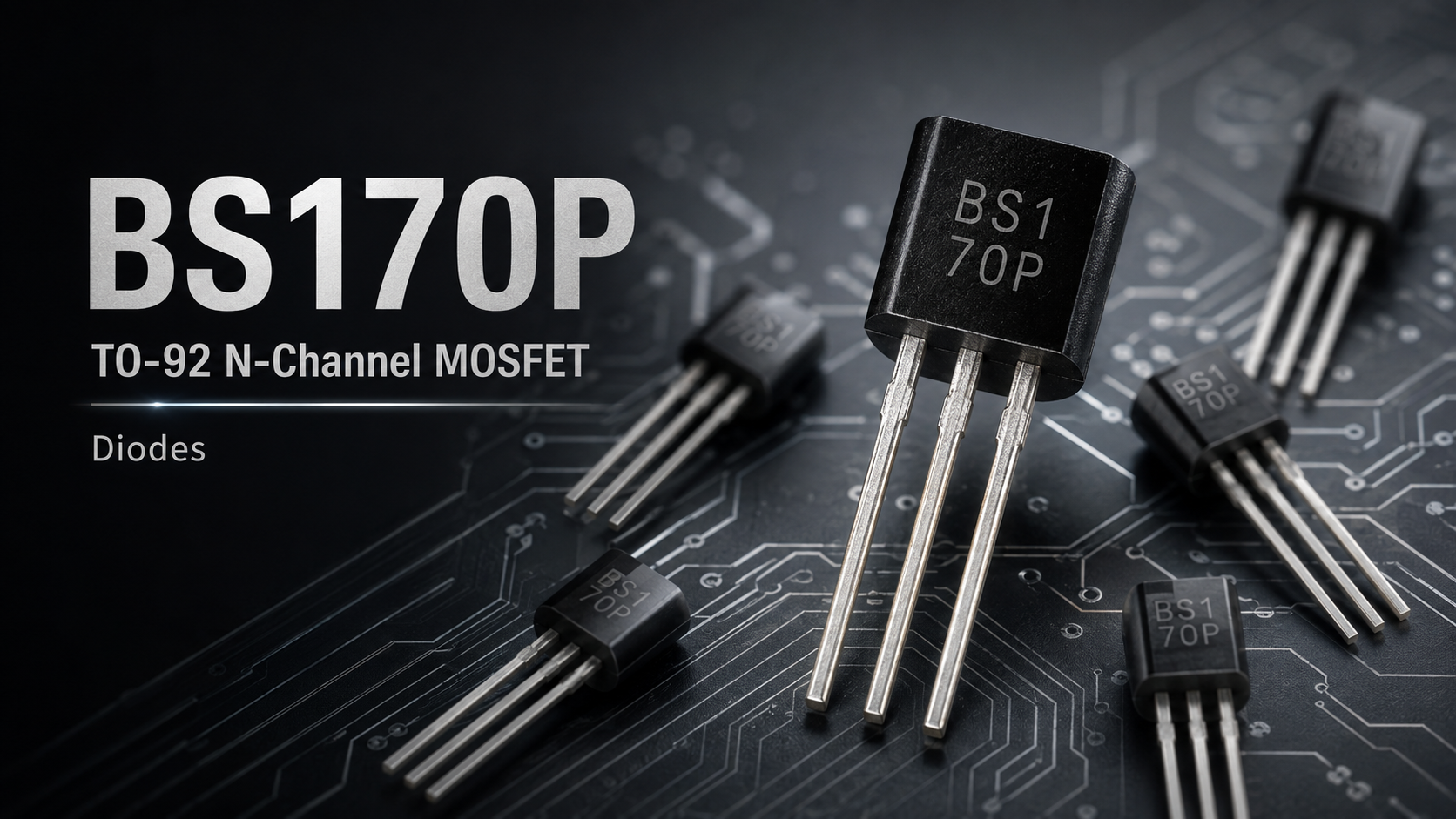
The BS170P is a compact N-channel enhancement-mode MOSFET from Diodes Incorporated, designed for low-power switching, signal control, driver circuits, and other applications where engineers need a simple through-hole transistor. With a drain-source voltage rating of 60 V, a maximum continuous drain current of 270 mA, and a familiar TO-92 compatible package, the BS170P has been widely used in prototypes, control boards, educational circuits, industrial equipment, and legacy electronic designs.
Although modern power MOSFETs often offer much lower resistance and higher current capability, the Diodes BS170P still has practical value. Its strength is not extreme power. Instead, it offers a useful combination of small size, easy PCB mounting, voltage-controlled operation, low gate current, and straightforward circuit integration.
This guide explains the BS170P MOSFET from a practical engineering point of view. We will look at BS170P specifications, operating principles, TO-92 packaging, pinout considerations, switching applications, testing methods, replacement selection, common design mistakes, and the situations where this small MOSFET still makes sense.
BS170P Search Guide: Find the Answer You Need Fast
People searching for BS170P are not always looking for the same thing. Some need the datasheet, some need the pinout, and others are trying to repair a board or find a practical substitute. The quick map below connects the most common BS170P search queries with the engineering question behind them.
What Is the BS170P?
The BS170P is an N-channel enhancement-mode vertical DMOS field-effect transistor. In simpler words, it is an electronic switch controlled mainly by voltage at its gate terminal.
Unlike a bipolar transistor that normally needs continuous base current, a MOSFET has an insulated gate. The gate therefore requires very little steady-state current. A suitable gate-to-source voltage creates a conductive channel between the drain and source terminals, allowing current to flow through the device.
This characteristic makes the BS170P transistor useful for circuits controlled by logic signals, timers, microcontrollers, sensors, analog stages, and other low-current control sources.
The device belongs to the small-signal MOSFET category rather than the high-power MOSFET category. That difference is important. The BS170P can control many useful loads, but it should not automatically be treated as a motor-power transistor simply because it is called a MOSFET.
BS170P Key Specifications
Understanding the numbers in a BS170P datasheet is more useful than simply memorizing them. Each specification tells you something about how the transistor should be used in a real circuit.
| Parameter | BS170P Specification | Practical Meaning |
|---|---|---|
| Manufacturer | Diodes Incorporated | Original manufacturer of the referenced BS170P device |
| Device Type | N-Channel Enhancement MOSFET | Normally off when gate-source voltage is near zero |
| Drain-Source Voltage | 60 V | Maximum VDS rating requires adequate design margin |
| Continuous Drain Current | 270 mA at specified conditions | Suitable mainly for low-current loads |
| RDS(on) | Up to 5 Ω at VGS = 10 V | Conduction loss can become important as current increases |
| Gate-Source Voltage | ±20 V maximum | Gate voltage must stay within this absolute limit |
| Gate Threshold Voltage | Up to 3 V | Threshold indicates the start of conduction, not full enhancement |
| Power Dissipation | 625 mW under specified conditions | Thermal conditions must be considered carefully |
| Input Capacitance | About 60 pF typical | Relatively easy to drive in low-power switching circuits |
| Package | TO-92 compatible / E-Line | Through-hole package suitable for hand assembly and prototyping |
Why the 60 V Rating Matters
One of the most noticeable BS170P specifications is its 60 V drain-source voltage rating. This gives the transistor more voltage capability than many low-voltage logic MOSFETs used only in 3.3 V or 5 V systems.
However, a 60 V MOSFET should not automatically be operated continuously at exactly 60 V. Real circuits can generate switching spikes, inductive kickback, supply variations, and electrical noise. Good engineering practice leaves voltage margin between normal circuit voltage and the transistor's absolute maximum rating.
For example, a nominal 12 V or 24 V control circuit can often be a much more comfortable environment for a 60 V device than a circuit that normally operates close to 60 V.
This is especially important when the load is inductive. Relays, coils, small solenoids, and motors can generate high-voltage transients when current is interrupted. A suitable flyback diode, clamp, snubber, or transient suppression method may be required.
Understanding the 270 mA Drain Current Rating
Searches for BS170P current rating often lead to the 270 mA continuous drain current figure. That number is useful, but it should not be interpreted as a promise that every circuit can safely run the transistor continuously at 270 mA.
Current capability depends on several conditions, including ambient temperature, PCB layout, gate voltage, drain-source resistance, airflow, duty cycle, and total power dissipation.
This is one reason why engineers should evaluate MOSFET power using more than the current rating alone.
A simple conduction-loss estimate is:
If the current rises, power loss increases with the square of current. Because the BS170P has an on-resistance measured in ohms rather than milliohms, its conduction loss can become significant surprisingly quickly.
For this reason, the BS170P N-channel MOSFET is usually more comfortable in low-current switching applications than in circuits that require maximum current continuously.
BS170P RDS(on): Why 5 Ohms Is Important
The maximum BS170P RDS(on) is specified as 5 Ω under a 10 V gate-drive condition at the stated test current. Compared with modern power MOSFETs, 5 Ω sounds high, and it is.
That does not make the BS170P a bad transistor. It simply tells you what type of jobs it was designed to perform.
Consider a load drawing only 20 mA. Even several ohms of resistance may create a manageable voltage drop and power loss. But if the same transistor is expected to drive hundreds of milliamps continuously, conduction losses become much more important.
This leads to one of the most useful design insights about the BS170P: voltage capability is one of its advantages, while ultra-low conduction resistance is not.
That makes it better suited to signal switching, small relays, LED control, level shifting, bias control, and other moderate or low-current applications than to high-efficiency power conversion.
Is the BS170P a Logic-Level MOSFET?
This question deserves special attention because it is easy to misunderstand MOSFET threshold voltage.
The BS170P gate threshold voltage can be as high as approximately 3 V. But threshold voltage does not mean the transistor is fully turned on at that voltage.
VGS(th) is measured at a very small drain current. It mainly tells you when the channel starts to conduct.
The important BS170P on-resistance specification, by contrast, is given at a gate-source voltage of 10 V.
Therefore, designers should not assume that a 3.3 V microcontroller output will drive the BS170P into the same low-resistance state specified at VGS = 10 V.
A 5 V logic output may operate the device in some low-current circuits, but the actual drain current, voltage drop, temperature, and required switching performance must be evaluated.
If guaranteed low RDS(on) at 2.5 V, 3.3 V, or 4.5 V is important, a modern logic-level MOSFET with explicit resistance specifications at those gate voltages may be the better choice.
BS170P TO-92 Package
The BS170P TO-92 package is one of the reasons this device remains recognizable. TO-92 is a small through-hole transistor package commonly used in discrete semiconductor circuits.
Through-hole components have several practical advantages. They are easy to handle with standard tools, convenient for breadboards and prototype boards, and simple to replace during repair work.
This makes the BS170P TO-92 MOSFET attractive for laboratories, training projects, industrial repairs, low-volume assembly, test fixtures, and legacy PCB replacement.
Surface-mount components are usually better for high-density automated production, but a TO-92 MOSFET can still be more convenient when accessibility and manual replacement matter more than PCB area.
BS170P Marking, E-Line Package and TO-92 Identification
The package code matters because "TO-92" describes a physical package family, not a universal electrical pin order. Two transistors can look almost identical while using different Gate, Drain and Source arrangements. For production, repair, or distributor incoming inspection, compare the actual body marking and the manufacturer's package drawing rather than relying only on a generic TO-92 photo.
The historical Diodes ordering information also distinguishes straight-lead and joggled-lead versions. That detail can matter for automated insertion, legacy PCB fit and replacement stock. When sourcing BS170P for an existing board, verify the exact orderable part number, lead style and packaging rather than assuming every BS170P listing is mechanically identical.
BS170P Pinout: Check Before Installing
When searching for a BS170P pinout, avoid assuming that every transistor in a TO-92 body has the same lead arrangement.
The three MOSFET terminals are:
- Gate (G): controls the conductivity of the MOSFET.
- Drain (D): commonly connects toward the load in a low-side switching circuit.
- Source (S): commonly connects toward ground in a low-side N-channel circuit.
The mechanical drawing and orientation shown in the manufacturer datasheet should always be checked before PCB design or installation. Package shape alone is not enough to determine lead order.
This becomes especially important when looking for a BS170P replacement. A replacement MOSFET can have suitable electrical ratings but a different physical pin arrangement.
A transistor with the wrong lead order may appear similar on paper yet fail immediately when installed in an existing board.
How Does the BS170P Work?
The BS170P is an enhancement-mode MOSFET, meaning it is normally off when the gate-source voltage is approximately zero.
As the gate voltage rises relative to the source, an electric field forms inside the transistor and creates a conducting channel. Current can then flow between drain and source.
Because the gate is insulated, the transistor does not require continuous DC gate current in the same way that a bipolar junction transistor requires base current.
However, the gate behaves partly like a small capacitor. Whenever the MOSFET switches on or off, this capacitance must be charged or discharged.
For slow switching, this usually requires very little effort. At higher switching frequencies, gate drive strength and switching time become increasingly important.
Typical BS170P Applications
The combination of a 60 V rating, low steady-state gate current, compact TO-92 package, and moderate switching capability gives the Diodes BS170P a useful range of applications.
1. Small Relay Driver Circuits
The BS170P can be used as a low-side switch for suitable low-current relay coils. A controller drives the gate, while the transistor switches current through the relay.
Because a relay coil is inductive, a flyback diode is normally placed across the coil to absorb the voltage generated when the MOSFET turns off.
2. LED Switching
A BS170P circuit can control low-current LEDs or small LED groups. The MOSFET allows a low-current control signal to switch a separate load current.
A suitable resistor or current-control circuit must still be used with the LED. The MOSFET does not replace LED current limiting.
3. Microcontroller Output Expansion
A microcontroller GPIO pin cannot directly drive every external load. A MOSFET can provide isolation between the low-current digital output and a somewhat larger load.
The BS170P may be useful when the required load current is low enough and the available gate voltage provides acceptable MOSFET performance.
For 3.3 V designs, however, designers should compare it carefully with dedicated logic-level MOSFETs.
4. Signal Switching
The BS170P can be used for switching or controlling electrical signals in instrumentation, test equipment, hobby electronics, and simple analog circuits.
Because it is voltage controlled, it can be convenient in circuits where the control source cannot provide significant current.
5. Level Shifting and Interface Circuits
Small N-channel MOSFETs are commonly found in interface circuits. Depending on the exact topology and signal requirements, a device such as the BS170P can assist with switching between different voltage domains.
Designers should still consider switching speed, threshold voltage, body diode behavior, and voltage levels before choosing it for bidirectional interfaces.
6. Educational and Prototype Circuits
TO-92 devices remain popular for teaching because students can easily identify, insert, remove, and measure them.
A BS170P transistor can demonstrate MOSFET concepts such as threshold voltage, gate control, drain current, switching operation, body diode behavior, and load control without requiring tiny surface-mount packages.
7. Legacy Equipment Maintenance
This may now be one of the most important applications for BS170P.
Many industrial boards, instruments, controllers, older consumer products, and custom electronic systems were designed years ago. Repairing those systems does not always mean redesigning the entire circuit with the newest transistor.
When the original BOM specifies BS170P, maintaining the same device can reduce validation work and minimize unexpected changes in circuit behavior.
How to Use BS170P as a Low-Side Switch
A common BS170P application uses the transistor as a low-side switch.
In this circuit:
- The source connects to circuit ground.
- The drain connects to the negative side of the load.
- The positive side of the load connects to its supply voltage.
- The gate receives the control signal.
- A gate pulldown resistor may be used to keep the MOSFET off when the controller output is floating.
When the gate voltage rises sufficiently above the source, the MOSFET turns on and current flows through the load.
When the gate returns to approximately the same voltage as the source, the MOSFET switches off.
For inductive loads, add suitable transient protection. For sensitive digital circuits, also consider gate resistance, grounding, switching noise, and power-supply decoupling.
Why a Gate Pulldown Resistor Is Useful
The MOSFET gate can retain electrical charge because it behaves like a capacitor. If a microcontroller pin becomes high impedance during reset or startup, the gate can temporarily float.
A floating gate can cause unpredictable switching.
A resistor connected between gate and source gives the gate charge a controlled path to discharge, helping keep the BS170P off until the control circuit intentionally turns it on.
Values such as tens or hundreds of kilohms are common in many low-frequency designs, although the correct value depends on the circuit.
This small component can significantly improve startup behavior and circuit reliability.
How to Test a BS170P MOSFET
Users searching for how to test BS170P often want to determine whether a device removed from a board is still working.
A digital multimeter with diode-test mode can provide a basic check.
Step 1: Identify the Terminals
Confirm gate, drain, and source using the correct BS170P datasheet. Do not identify the pins only by comparing the package with another TO-92 transistor.
Step 2: Discharge the Gate
Briefly connect gate and source together. This removes stored gate charge and helps place the MOSFET in its off state.
Step 3: Check for a Short Circuit
Measure between drain and source in both directions. The readings should not behave like a permanent short circuit.
Remember that an N-channel MOSFET contains an internal body diode, so one polarity can show diode-like behavior.
Step 4: Charge the Gate
Depending on the multimeter and test arrangement, applying a positive voltage from gate to source can charge the gate and make the MOSFET conduct.
Step 5: Discharge the Gate Again
Short gate to source again. Drain-source conduction caused by the gate charge should disappear.
This method is useful for a basic functional check, but it does not verify every specification. A transistor can pass a simple multimeter test and still fail under voltage, current, temperature, or high-frequency conditions.
Common BS170P Failure Symptoms
MOSFET failures are not always visually obvious. A damaged BS170P may look normal from the outside.
Possible symptoms include:
- Permanent drain-to-source short circuit.
- Load remains on even when the gate signal is low.
- Load never turns on.
- Unexpected voltage drop across the MOSFET.
- Excessive heating at moderate current.
- Intermittent operation after electrical overstress.
- Gate leakage that causes unstable switching.
When troubleshooting, also inspect the surrounding circuit. A failed flyback diode, incorrect gate drive, damaged resistor, excessive load current, power-supply transient, or PCB fault can damage the replacement transistor again.
BS170P Replacement and Equivalent Selection
There is no universal answer to the question, "What is the best BS170P equivalent?" The correct replacement depends on the original circuit.
When comparing a BS170P replacement, examine at least the following:
- N-channel MOSFET architecture.
- Drain-source voltage rating.
- Continuous and pulsed drain-current capability.
- Gate-source voltage limits.
- RDS(on) at the actual gate voltage used in the circuit.
- Threshold characteristics.
- Input and output capacitance.
- Switching speed.
- Power dissipation and thermal limits.
- TO-92 or other required package.
- Gate, drain, and source pin arrangement.
A replacement with a lower RDS(on) can sometimes reduce conduction loss, but that alone does not guarantee compatibility. Different gate charge or capacitance can change switching behavior, while a different threshold characteristic may affect analog circuits.
For repair work, mechanical compatibility can be just as important as electrical compatibility.
BS170 vs BS170P: Are They Always the Same?
The names BS170 and BS170P are often used in searches as though they describe one universal component. In practice, device suffixes and ordering codes can depend on the manufacturer.
Two components carrying similar BS170 names may have broadly similar functions while differing in package details, ordering format, electrical limits, manufacturing status, or pin configuration.
For this reason, a search for BS170 vs BS170P should end with a comparison of the actual manufacturer datasheets rather than a comparison of names alone.
If you are replacing the Diodes Incorporated BS170P, verify the exact part number and package before purchase.
BS170P vs BS170F: Package and Electrical Differences
A useful same-family comparison is BS170P vs BS170F. Both are 60 V N-channel enhancement-mode MOSFETs from Diodes with a maximum RDS(on) specification of 5 Ω at VGS = 10 V, but their package and current / power figures are different. This means BS170F should not be treated as a drop-in replacement for a BS170P TO-92 board.
| Comparison | BS170P | BS170F | Why It Matters |
|---|---|---|---|
| Package | E-Line / TO-92 compatible, through-hole | SOT23, surface-mount | They are mechanically different and are not direct PCB drop-in substitutes. |
| VDS | 60 V | 60 V | Voltage class is similar, but voltage alone is not enough to establish equivalence. |
| Continuous ID | 0.27 A at stated conditions | 0.15 A at stated conditions | Current capability differs, so load requirements must be checked. |
| RDS(on) | 5 Ω max at VGS = 10 V | 5 Ω max at VGS = 10 V | Similar headline on-resistance does not make the devices interchangeable. |
| Power Dissipation | 0.625 W at stated conditions | 0.33 W at stated conditions | Package and thermal environment change how much heat the device can handle. |
| Best Fit | Through-hole prototypes, repair and legacy boards | Compact surface-mount layouts | Select according to PCB format, thermal needs and lifecycle requirements. |
BS170P vs Modern Logic-Level MOSFET
The BS170P was not designed to compete with today's lowest-resistance MOSFETs.
| Design Requirement | BS170P | Modern Logic-Level MOSFET |
|---|---|---|
| Through-hole prototyping | Very convenient | Depends on available package |
| 60 V capability | Available | Many options available |
| Very low RDS(on) | Not its main strength | Often much better |
| Guaranteed 3.3 V gate drive | Must be evaluated carefully | Often explicitly specified |
| Legacy board replacement | Strong fit when originally specified | Requires compatibility review |
| High-current motor control | Generally not ideal | Many better choices exist |
| Simple low-current switching | Good application | Also suitable |
The key lesson is that "newer" and "better" depend on the application.
For a new battery-powered 3.3 V product, a modern logic-level MOSFET may provide better efficiency. For repairing an existing board designed around the BS170P TO-92, changing the transistor type may create unnecessary engineering work.
Important Thermal Design Considerations
The BS170P has a maximum power-dissipation figure of 625 mW under specified conditions, but real operating temperature depends strongly on the environment.
As semiconductor temperature rises, electrical behavior can change. Excessive junction temperature reduces reliability and can eventually destroy the device.
For continuous operation, calculate estimated conduction loss and consider ambient temperature. If the transistor is switching frequently, switching loss may also need to be included.
Do not treat the maximum power rating as a target operating point. Reliable designs normally use reasonable thermal margin.
Common BS170P Design Mistakes
Using Threshold Voltage as the Turn-On Voltage
This is probably the most common misunderstanding. A MOSFET beginning to conduct at its threshold voltage does not mean it is fully enhanced.
Always examine the gate voltage associated with the RDS(on) specification.
Ignoring RDS(on)
Five ohms can be almost irrelevant at extremely small currents but significant at higher currents. Calculate the expected voltage drop and power.
Driving an Inductive Load Without Protection
A relay or coil can produce a voltage spike when turned off. Suitable suppression protects the MOSFET and surrounding electronics.
Assuming Every TO-92 Pinout Is Identical
TO-92 describes a package style, not a universal lead assignment. Verify the datasheet.
Leaving the Gate Floating
A floating MOSFET gate can collect charge and cause unpredictable operation. Use appropriate biasing such as a gate-to-source pulldown where necessary.
Choosing a Replacement by Current Rating Alone
Voltage, RDS(on), gate-drive voltage, thermal behavior, package, pinout, switching characteristics, and circuit function all matter.
Is BS170P Still Suitable for New Designs?
This question requires some context.
Diodes Incorporated currently identifies the BS170P as a device that is not recommended for new design. This does not mean existing BS170P components suddenly stop functioning or that every circuit using one must be redesigned.
Instead, it is an important lifecycle consideration.
For a new product expected to remain in production for many years, engineers should investigate actively supported alternatives before freezing the BOM.
For legacy equipment, service inventories, replacement boards, educational projects, and existing validated products, genuine BS170P devices may continue to have practical value while supply is available.
This distinction between new design and existing design support is important. Component lifecycle management is not only about electrical specifications; it is also about availability, qualification cost, redesign risk, and long-term supply strategy.
How to Choose a BS170P Supplier
When purchasing BS170P MOSFETs, especially for repair or production use, component traceability matters.
A reliable supplier should clearly identify:
- Manufacturer name.
- Exact manufacturer part number.
- Package type.
- Quantity and packaging format.
- Product lifecycle information when available.
- Datasheet reference.
- Lot or traceability information for professional applications.
For electronic components that have been on the market for many years, buyers should also consider storage conditions, solderability, labeling consistency, and source reliability.
The lowest unit price is not always the lowest total cost if incoming inspection, rework, counterfeit risk, or production downtime becomes a problem.
When Does BS170P Make the Most Sense?
The BS170P is particularly practical when the circuit needs a compact through-hole N-channel MOSFET and the load current is relatively small.
Good use cases can include:
- Legacy circuit-board repair.
- Low-current relay control.
- Small indicator or LED switching circuits.
- Laboratory fixtures.
- Prototype boards.
- Educational electronics.
- Signal switching.
- Simple interface circuits.
- Industrial equipment maintenance.
- Existing products originally qualified with BS170P.
Applications demanding very low conduction loss, large continuous current, high-efficiency power conversion, or guaranteed operation from a low 3.3 V gate signal often benefit from a newer MOSFET specifically optimized for those requirements.
Frequently Asked Questions About BS170P
What type of transistor is the BS170P?
The BS170P is an N-channel enhancement-mode MOSFET. It is normally off when gate-source voltage is near zero and turns on when sufficient positive gate voltage is applied relative to the source.
Who manufactures the BS170P?
The device discussed in this guide is the BS170P from Diodes Incorporated.
What package does the BS170P use?
The Diodes BS170P uses an E-Line package that is compatible with the familiar TO-92 through-hole package.
What is the BS170P drain-source voltage?
The device has a 60 V drain-source voltage rating. Engineers should still provide appropriate design margin and protection against switching transients.
What is the maximum continuous drain current?
The published continuous drain-current rating is 270 mA under specified conditions. Actual safe current depends on thermal conditions, gate drive, resistance, duty cycle, and the complete circuit design.
What is BS170P RDS(on)?
The maximum on-state resistance is specified at up to 5 Ω with VGS = 10 V under the manufacturer's stated test conditions.
Can a 3.3 V microcontroller drive BS170P?
The gate may begin turning the transistor on at a few volts, but the main low-resistance specification is not guaranteed at 3.3 V. If reliable low-resistance switching from a 3.3 V GPIO is required, compare the BS170P with a MOSFET specifically rated for 2.5 V or 3.3 V gate drive.
Can BS170P be used with Arduino?
It may be used in suitable low-current Arduino switching circuits, but designers should calculate load current and voltage drop rather than assuming full enhancement from logic voltage. A dedicated logic-level MOSFET may be better for higher-current loads.
Can BS170P drive a motor?
It may control a very small motor if voltage, current, starting current, thermal conditions, and transient protection are all within safe limits. For typical power motor applications, a lower-resistance and higher-current MOSFET is usually preferable.
Can BS170P drive a relay?
Yes, it can control suitable low-current relay coils when the circuit meets its electrical limits. A flyback diode is normally required across a DC relay coil.
How do I find the correct BS170P pinout?
Use the Diodes Incorporated datasheet and pay attention to the package viewing direction. Do not assume another BS170 or TO-92 transistor uses an identical lead order.
What should I check when buying a BS170P equivalent?
Compare VDS, drain current, RDS(on), gate-drive requirements, VGS limits, capacitance, power dissipation, operating temperature, package, and pinout. For replacement work, verify that the substitute behaves correctly in the actual circuit.
Is BS170P suitable for high-frequency switching?
The device can switch relatively quickly and has modest input capacitance, but suitability depends on frequency, gate-drive impedance, load current, switching losses, and circuit layout. Modern MOSFETs may offer better performance in demanding high-frequency converters.
Why does my BS170P become hot?
Common reasons include excessive drain current, insufficient gate voltage, high RDS(on), excessive switching losses, inadequate thermal conditions, or operation outside the intended design range.
What is the difference between a BS170P and a bipolar transistor?
A bipolar transistor is primarily current controlled, while the BS170P MOSFET is primarily voltage controlled. MOSFET gates draw very little steady-state current, although the gate capacitance must be charged and discharged during switching.
BS170P Design Checklist
Before placing the BS170P into a circuit, answer these questions:
- Is the maximum drain-source voltage comfortably below the device limit?
- Are switching spikes and inductive transients controlled?
- Is the continuous load current reasonable for the device?
- What is the expected RDS(on) at the actual gate voltage?
- How much conduction power will the MOSFET dissipate?
- Is the gate driven high enough for the required current?
- Does the gate need a pulldown resistor?
- Is the load inductive?
- Is a flyback diode or other clamp required?
- Has the exact BS170P pinout been verified?
- Is the TO-92 package compatible with the PCB?
- Is component lifecycle acceptable for the project?
Answering these questions before production can prevent many of the failures that are incorrectly blamed on the MOSFET itself.
Final Thoughts on the Diodes BS170P TO-92 MOSFET
The BS170P is a good example of why component selection should be based on circuit requirements rather than impressive-looking headline specifications.
It offers a useful 60 V N-channel MOSFET architecture in an easy-to-handle TO-92 compatible package, with a maximum continuous drain current of 270 mA and low steady-state gate-current requirements.
At the same time, its RDS(on) of up to 5 Ω at a 10 V gate drive makes it very different from modern low-resistance power MOSFETs. It should therefore be viewed primarily as a small-signal and low-current switching device rather than a high-current power switch.
For engineers maintaining existing hardware, technicians repairing older equipment, distributors supporting legacy BOMs, students learning MOSFET operation, and developers building simple through-hole circuits, the Diodes BS170P can still be a useful device.
For completely new commercial designs, lifecycle status and newer MOSFET alternatives deserve careful consideration. A newer device may provide lower RDS(on), better 3.3 V or 5 V gate-drive performance, higher current capability, or stronger long-term supply support.
The best approach is simple: read the BS170P datasheet, understand the actual load and gate voltage, calculate power loss, confirm the BS170P pinout, protect the transistor from transients, and compare alternatives based on the complete circuit rather than one specification.
When used within the right operating conditions, the BS170P demonstrates an important engineering principle: a component does not need extreme current ratings or ultra-low resistance to remain useful. It only needs to be correctly matched to the job.