

PC817X3NIP1B Optocoupler: Specs, CTR and Design Guide
A high-isolation single-channel phototransistor optocoupler with C-rank current transfer ratio for power, control and industrial signal isolation.
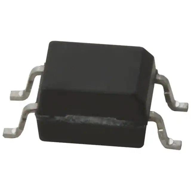
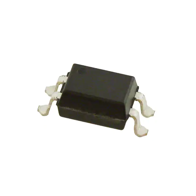
PC817X3NIP1B combines an infrared LED and a phototransistor inside an electrically isolated 4-pin SMD gull-wing package. It provides 5kVrms input-to-output isolation and a controlled CTR rank of 200% to 400% at IF=5mA and VCE=5V.
Why PC817X3NIP1B Is More Than a Generic PC817
PC817 is one of the best-known names in basic optocouplers, but a design engineer should not treat every PC817 ordering code as identical. The full part number matters. The PC817X3NIP1B identifies a particular lead-free, surface-mount version with a selected current-transfer-ratio rank. That selection is useful because CTR is one of the most important variables in a phototransistor optocoupler.
Inside the package, the input side contains an infrared emitting diode. When current flows through the LED, it produces light. A phototransistor on the output side detects that light and allows collector current to flow. There is no normal conductive path between the two sides. This optical barrier is what allows a low-voltage controller to sense or control another circuit while maintaining galvanic isolation.
The basic idea sounds simple, but the design value comes from controlling the details. The designer must choose LED current, output pull-up resistance, switching speed, noise margin and long-term CTR margin. The X3 rank helps because its transfer range is narrower than an unranked PC817 device. At the specified test point of IF=5mA and VCE=5V, the collector current for PC817X3NIP1B is 10mA to 20mA. In CTR language, that corresponds to about 200% to 400%.
This narrower range can make calculations easier. It does not mean the circuit should always be designed to draw 10mA or 20mA from the transistor. Real collector current is limited by the external load, supply voltage, transistor saturation and temperature. CTR is a transfer relationship, not a promise that the output can create unlimited current.
PC817X3NIP1B Key Specifications
| Parameter | PC817X3NIP1B Value | Design Meaning |
|---|---|---|
| Device Type | Phototransistor output optocoupler | Transfers a DC or switching signal through an optical barrier. |
| Number of Channels | 1 | One LED input and one phototransistor output path. |
| CTR Rank | C rank / 200% to 400% | At IF=5mA and VCE=5V, the X3 grade provides a tighter transfer range. |
| Collector Current at CTR Test | 10mA to 20mA | Specified for PC817X3NIP1B at IF=5mA, VCE=5V and Ta=25°C. |
| Isolation Voltage | 5.0kVrms | High galvanic isolation between LED input and transistor output. |
| Forward Current IF | 50mA max | Absolute maximum continuous LED current at the stated rating condition. |
| LED Forward Voltage | 1.2V typ, 1.4V max | Specified at IF=20mA and useful when calculating the LED series resistor. |
| LED Reverse Voltage | 6V max | Reverse stress across the input LED must remain controlled. |
| Collector-Emitter Voltage | 80V max | Maximum output-side VCEO rating. |
| Collector Current | 50mA max | Absolute maximum output transistor collector current. |
| VCE Saturation | 0.1V typ, 0.2V max | Specified at IF=20mA and IC=1mA. |
| Cut-Off Frequency | 80kHz typ | General-purpose signal isolation rather than high-speed digital transfer. |
| Rise Time | 4µs typ, 18µs max | Specified at VCE=2V, IC=2mA and RL=100Ω. |
| Fall Time | 3µs typ, 18µs max | Output transition time depends on load and operating point. |
| Operating Temperature | -30°C to +100°C | Useful across a broad range of control and power applications. |
| Storage Temperature | -55°C to +125°C | Absolute storage range when the device is not operating. |
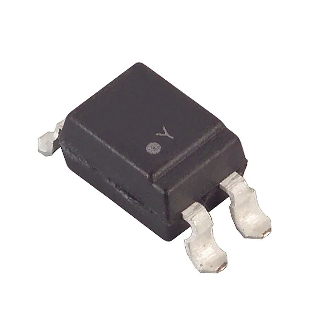
| Package / Case | 4-SMD, Gull Wing | The NIP1B product uses lead-formed surface-mount construction. |
| Mounting Type | Surface Mount | Designed for SMT PCB assembly. |
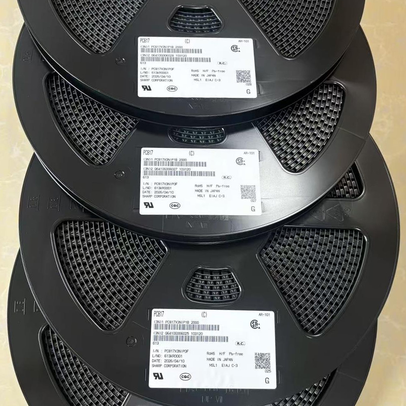
| Packaging | Tape and Reel | The referenced specification states 2000 devices per reel as the basic quantity. |
What Does the X3 CTR Rank Mean?
The X3 portion of PC817X3NIP1B is especially important because it defines the transfer rank. For this ordering code, the rank mark is C. At 25°C, with 5mA flowing through the input LED and 5V across the output transistor, the specified collector-current range is 10mA to 20mA. Dividing collector current by LED current gives a CTR range of 200% to 400%.
CTR is often explained as gain, but that description can lead to poor circuit decisions. An optocoupler is not a precision linear amplifier. CTR changes with LED current, temperature, device age and collector operating point. A 300% CTR does not mean that 5mA at the LED guarantees 15mA at the collector under every condition.
A better design method is to begin with the minimum guaranteed CTR that applies to the exact ordering code. For PC817X3NIP1B, that selected rank gives the designer more useful lower-bound information than a very wide generic PC817 CTR range.
Then calculate whether the output pull-up and logic threshold still work with that minimum transfer. After that, include extra margin for LED aging, temperature, supply tolerance and resistor tolerance.
How to Choose the PC817X3NIP1B LED Resistor
The input side behaves like an infrared LED, so it needs a current-limiting resistor. A useful first estimate is: R = (VIN − VF) / IF.
For example, if a 5V signal drives the optocoupler, the LED voltage is about 1.2V and the target LED current is 5mA, the resistor calculation is approximately: (5 − 1.2) / 0.005 = 760Ω.
A nearby standard resistor value can then be chosen after checking supply tolerance, LED forward-voltage tolerance and the required worst-case output current.
The 50mA input-current specification is an absolute maximum, not a recommended normal operating point. Driving an LED close to its maximum rating increases heat, power use and long-term light-output degradation.
The photocoupler documentation also warns that LED light output decreases with long operation and that variation becomes more important when LED current is set below about 1mA. Very low input current can save power, but the output circuit then needs enough CTR margin to remain reliable after aging.
How to Choose the Output Pull-Up Resistor
The phototransistor output is commonly wired as an open-collector style signal. The collector connects to a pull-up resistor and the emitter connects to output-side ground.
When the input LED is off, the pull-up holds the node high. When the LED turns on, the phototransistor sinks current and pulls the node low.
A smaller pull-up resistor creates more current and can produce a strong logic-low state, but it also requires more collector current from the optocoupler. A larger pull-up reduces current demand, but the output may rise more slowly because the resistor has to charge parasitic capacitance.
This is why CTR margin and switching speed should be designed together rather than treated as separate specifications.
Is PC817X3NIP1B a High-Speed Optocoupler?
No. PC817X3NIP1B is best treated as a general-purpose phototransistor optocoupler.
The specification gives a typical cut-off frequency of about 80kHz. At the defined response-time test point, typical rise time is about 4µs and typical fall time is about 3µs.
That performance is useful for power-supply feedback, status signals, PLC inputs, interlocks and many control circuits, but it is not intended for multi-megabit digital communications.
Another factor is phototransistor saturation. Driving the transistor deeply into saturation can store charge and increase turn-off time. More LED current can improve logic margin, while too much saturation can make the signal slower.
The correct operating point therefore depends on whether the application values low power, noise margin or response time most strongly.
Where Is PC817X3NIP1B Used?
The PC817 family is commonly used wherever two circuits need to exchange a relatively slow signal without sharing a direct electrical connection.
Typical applications include switching power supplies, office equipment, communication terminals, measuring equipment, machine tools, audio/video equipment and home appliances.
In a switching power supply, the optocoupler may carry feedback information between the low-voltage secondary side and the primary controller.
In industrial control equipment, it can isolate a field input from an MCU or PLC logic circuit. Motor-control systems can use it for fault, status and enable signals.
However, electrical isolation should not be confused with complete system protection. A 5kVrms isolation rating is a device dielectric test value. PCB creepage, clearance, surge protection, fusing, contamination level and applicable safety standards must still be considered.
PC817X3NIP1B Package: Why NIP1B Matters
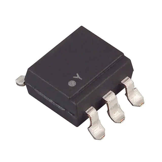
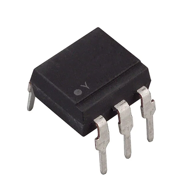
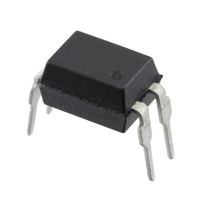
A common catalog mistake is to show PC817X3NIP1B as a normal four-pin through-hole DIP.
The basic PC817 family uses a DIP-style body, but the exact NIP1B ordering configuration uses formed leads for surface mounting.
Distributor data identifies PC817X3NIP1B as 4-SMD, Gull Wing with Surface Mount mounting.
The package body is approximately 6.5mm by 4.6mm, while the formed lead span is about 9.6mm in the referenced outline.
The four terminals remain simple: pin 1 is Anode, pin 2 is Cathode, pin 3 is Emitter and pin 4 is Collector.
Package/Case: 4-SMD, Gull Wing
Mounting Type: Surface Mount
Number of Channels: 1
Output Type: Phototransistor
PCB Layout Tips for PC817X3NIP1B
Do not route unnecessary copper or signal traces across the physical isolation region. System creepage and clearance must satisfy the actual working-voltage and safety requirements.
Calculate the input resistor using the complete input voltage and LED forward-voltage range rather than only typical values.
A very small resistor may demand more collector current than the worst-case CTR can provide. A very large resistor can slow the output transition.
If switching speed matters, do not force the phototransistor much deeper into saturation than required.
PC817X3NIP1B is the gull-wing lead-form version. Do not automatically use the straight-lead through-hole PC817 footprint.
Common PC817X3NIP1B Design Mistakes
- Using typical CTR as a guarantee: calculate the circuit with the specified minimum CTR.
- Confusing 5kV isolation with working voltage: the dielectric test rating is not the complete safety rating of the finished PCB.
- Driving the LED near 50mA continuously: 50mA is an absolute maximum rather than a recommended normal operating current.
- Ignoring LED aging: light output decreases over time, so a design with almost no CTR margin can become unreliable later.
- Using PC817 for high-speed communication: this phototransistor architecture is designed for general control rather than multi-megabit digital links.
- Ordering the wrong package: PC817 ordering codes can look very similar, but PC817X3NIP1B is a surface-mount gull-wing version.
When Is PC817X3NIP1B a Good Choice?
PC817X3NIP1B is a strong choice when a circuit requires high electrical isolation, moderate signal speed, a simple phototransistor output and a controlled CTR range.
It is especially useful for status signals, isolated feedback, slow logic interfaces, interlocks and power-electronics control.
The X3 CTR rank is useful when the very wide CTR spread of a generic optocoupler would make the output calculation difficult. Its 200% to 400% specified transfer range gives the designer a more focused operating window at the defined test point.
It is not the ideal device for very high-speed buses, precision analog isolation or fast power-switch gate driving. Those jobs normally require a high-speed optocoupler, linear optocoupler, isolated gate driver or digital isolator.
PC817X3NIP1B Sourcing and Lifecycle Notes
Availability should be checked with the actual supplier rather than inferred from one catalog.
Some distributors continue to list PC817X3NIP1B, while DigiKey currently marks the part as discontinued at DigiKey and no longer carried there. A distributor status does not automatically prove the universal manufacturer lifecycle status.
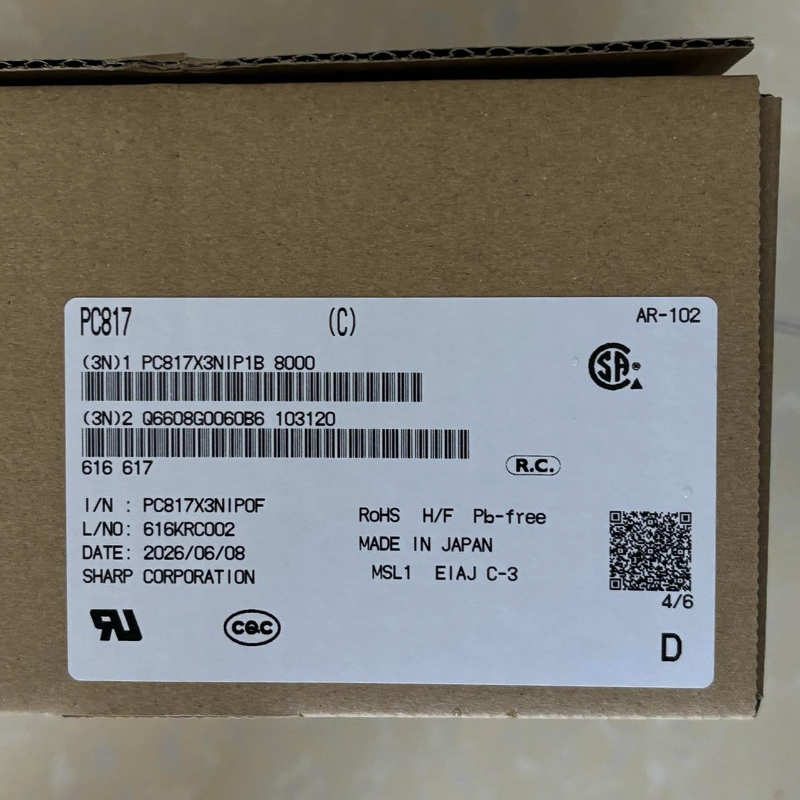
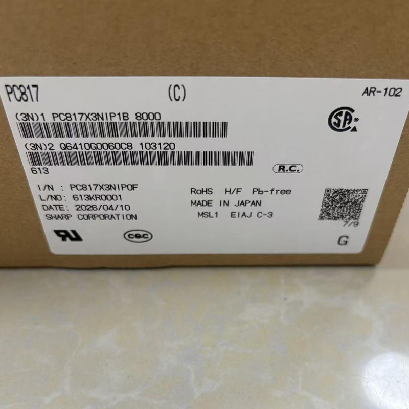
For sourcing, confirm the complete part number, X3/C CTR rank, 4-SMD gull-wing package, tape-and-reel configuration and manufacturer traceability.
The PC817X*NIP1B specification states that a reel basically contains 2000 pieces. The same reference lists UL recognition for PC817 under file E64380 and CSA approval. For safety-critical qualification, always check the latest approval documentation for the exact production source.
PC817X3NIP1B FAQ
What is PC817X3NIP1B?
What is the PC817X3NIP1B isolation voltage?
What CTR does PC817X3NIP1B have?
Is PC817X3NIP1B through-hole or surface mount?
What is the maximum PC817X3NIP1B output voltage?
What is the maximum LED forward current?
What is the typical PC817X3NIP1B LED forward voltage?
How fast is PC817X3NIP1B?
Can PC817X3NIP1B isolate a microcontroller signal?
Can PC817X3NIP1B be used in switching power supplies?
Is PC817X3NIP1B the same as every PC817 optocoupler?
Final Engineering Perspective
The PC817X3NIP1B is a simple component with a valuable engineering purpose: it transfers a control signal across an electrical isolation barrier using light instead of a direct conductive connection.
The most important feature of this exact ordering code is not only the familiar PC817 name. It is the combination of 5kVrms isolation, 80V phototransistor output, 200% to 400% C-rank CTR and 4-SMD gull-wing package.
Those details determine how the part should be calculated, mounted and sourced.
A robust circuit begins with minimum CTR, chooses a reasonable LED current, calculates the collector pull-up, includes margin for temperature and aging, and avoids deep transistor saturation when switching speed matters.
The PCB must also maintain the intended isolation boundary. An optocoupler can electrically separate two circuits, but the final equipment still needs correct creepage, clearance and protection design.
Used within those limits, PC817X3NIP1B remains a practical general-purpose isolation device for power supplies, industrial controllers, feedback circuits, embedded systems and many other low- to medium-speed applications.
.jpg)