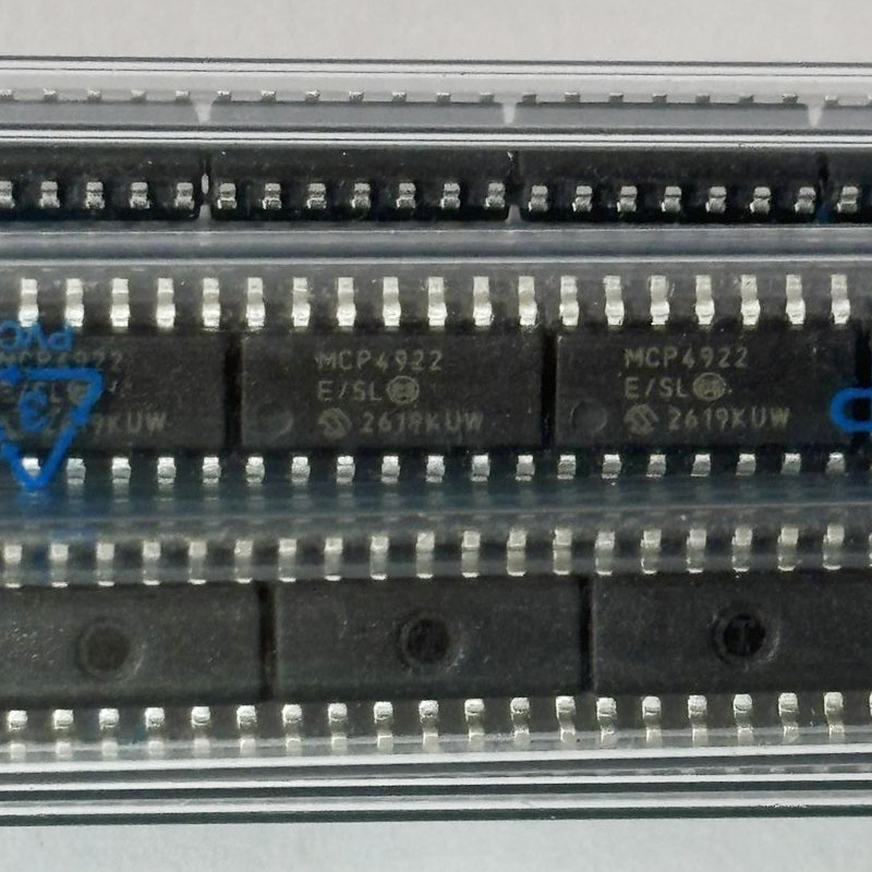
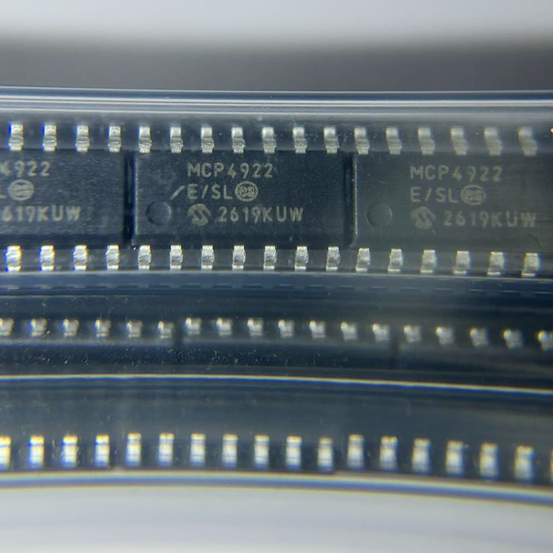
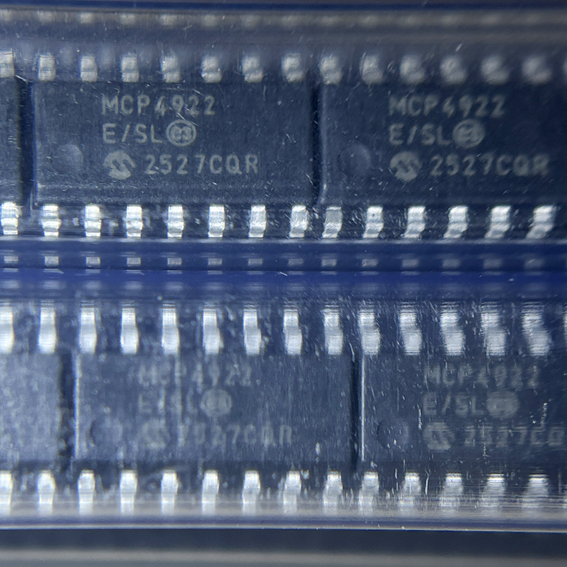
MCP4922-E/SL
IC DAC 12BIT V-OUT 14SOIC
Your reliable partner for semiconductor solutions. Flychip supports customers from R&D to mass production with electronic component supply, BOM sourcing, PCB, SMT and PCBA services.
- 20+
- Years Component Supply
- BOM
- Multi-Part Sourcing
- PCBA
- PCB / SMT Support
- Part No.:
- MCP4922-E/SL
- Manufacturer:
- Microchip Technology
- Category:
- Digital to Analog Converters (DAC)
- Package:
- 14-SOIC (0.154", 3.90mm Width)
- Datasheet:
- MCP4922-E/SL.pdf
- Description:
- IC DAC 12BIT V-OUT 14SOIC
- Quantity:


-
Quality Control
Supplier review, channel management and product verification before delivery.
-
Global Channels
International chip manufacturer and well-known distributor sourcing network.
-
BOM to Production
Component supply support from R&D prototype to mass production.
-
PCB / SMT / PCBA
Integrated manufacturing support to accelerate product development and delivery.
Product Details
MCP4922-E/SL 12-Bit Dual SPI DAC: Complete Design and Application Guide
The MCP4922-E/SL is a dual-channel, 12-bit digital-to-analog converter from Microchip Technology. It is designed for systems that need two accurate analog voltage outputs controlled through a simple SPI interface. With a compact 14-pin SOIC package, external voltage reference inputs, selectable output gain, fast settling, and simultaneous dual-channel updates, the MCP4922-E/SL is a practical choice for industrial control, sensor calibration, test equipment, motor control, waveform generation, and embedded electronics.
One reason the MCP4922-E/SL remains useful is that it gives designers direct control over the analog reference voltage. Unlike DACs that depend only on a fixed internal reference, the MCP4922 allows the reference source to be selected according to the accuracy, noise, and voltage range required by the application. This gives engineers more freedom when designing precision analog systems.
The device combines 12-bit resolution, two independently controlled DAC channels, SPI communication up to 20 MHz, rail-to-rail output capability, selectable 1x or 2x output gain, and a typical settling time of about 4.5 µs. The E temperature grade is intended for operation from -40°C to +125°C, while the SL suffix identifies the 14-lead narrow SOIC package.
What Is the MCP4922-E/SL?
The MCP4922-E/SL is a dual 12-bit voltage-output DAC. A DAC converts a digital number generated by a microcontroller, processor, FPGA, or other digital controller into a corresponding analog voltage.
A 12-bit DAC provides 4096 possible digital code levels, ranging from 0 to 4095. This gives much finer voltage adjustment than an 8-bit DAC with only 256 levels or a 10-bit DAC with 1024 levels.
The MCP4922 contains two DAC channels, normally identified as DAC A and DAC B. Each channel has its own voltage output and its own external reference input. This architecture makes it possible to create two related analog outputs from one IC while still allowing flexibility in the reference and output range.
For example, one channel could generate an adjustable control voltage while the second channel sets an offset, threshold, reference, or calibration level. In a motor control design, one output might establish a speed reference while the other controls torque or another analog parameter.
MCP4922-E/SL Key Specifications
| Parameter | MCP4922-E/SL |
|---|---|
| Manufacturer | Microchip Technology |
| Device Type | Digital-to-Analog Converter |
| Resolution | 12-bit |
| Number of DAC Channels | 2 |
| Digital Interface | SPI Compatible |
| Maximum SPI Clock | 20 MHz |
| Supply Voltage | 2.7 V to 5.5 V |
| Voltage Reference | External VREFA and VREFB |
| Output Gain | Selectable 1x or 2x |
| Typical Settling Time | 4.5 µs |
| Output Type | Buffered Voltage Output |
| Operating Temperature | -40°C to +125°C |
| Package | 14-Pin SOIC |
| Part Number | MCP4922-E/SL |
Understanding the MCP4922-E/SL Part Number
The ordering code MCP4922-E/SL contains useful information about the product configuration.
- MCP4922 identifies the dual-channel 12-bit DAC family.
- E identifies the extended operating temperature range.
- SL identifies the 14-lead narrow SOIC package.
The E temperature grade supports environments from approximately -40°C to +125°C. This makes the device suitable not only for general electronics but also for many industrial systems where temperatures may be wider than normal indoor consumer conditions.
The SOIC package is also useful in production because it provides a good balance between board size and ease of assembly. Compared with very small leadless packages, SOIC pins are relatively easy to inspect, solder, prototype, and rework.
Why 12-Bit Resolution Matters
Resolution determines how many individual voltage levels a DAC can generate. Since the MCP4922-E/SL is a 12-bit device, it provides:
212 = 4096 digital levels
Suppose a design uses a 4.096 V reference and unity gain. The theoretical step size is approximately:
4.096 V / 4096 = 1 mV per step
This is convenient because each increase in digital code represents roughly one millivolt. A code around 2048 would therefore produce approximately half of the selected full-scale range under ideal conditions.
The real accuracy of a system depends on more than resolution. Reference accuracy, reference noise, PCB layout, power supply quality, output loading, gain error, offset error, temperature, and DAC linearity all influence the final analog voltage.
This distinction is important. A 12-bit number does not automatically mean that every circuit will achieve perfect 12-bit system accuracy. Good analog design around the MCP4922-E/SL is still required.
Dual DAC Channels Provide More Design Flexibility
One of the biggest advantages of the MCP4922-E/SL compared with a single-channel DAC is its two-output architecture.
Instead of installing two separate DAC ICs, a designer can control two analog outputs through one SPI-connected component. This can reduce component count, board space, firmware complexity, and sourcing requirements.
The two channels are particularly useful when signals must operate as a pair. Examples include:
- Two-axis control systems
- Offset and gain adjustment
- Dual bias voltage generation
- Motor speed and torque references
- Two-channel test equipment
- Sensor excitation and calibration
- Analog threshold control
- Programmable voltage references
- Low-frequency waveform generation
An important feature is the LDAC pin. The device uses double-buffered registers, so digital values can first be loaded and then transferred to the DAC outputs together. This allows DAC A and DAC B to change at essentially the same update event instead of one output changing noticeably before the other.
That synchronized behavior can be valuable in systems where the relationship between two analog signals matters more than simply generating two independent voltages.
How the SPI Interface Works
The MCP4922-E/SL communicates through an SPI-compatible serial interface. Important digital control signals include CS, SCK, and SDI.
The microcontroller sends a 16-bit command containing both configuration information and DAC data. The command determines which DAC channel receives the data, how the voltage reference input is handled, whether 1x or 2x gain is selected, whether the selected channel is active, and what 12-bit digital value should be converted.
SPI is especially useful in embedded systems because it is simple, widely supported, and fast. Most modern microcontrollers include hardware SPI peripherals, so firmware can update the MCP4922 with little CPU overhead.
With clock support up to 20 MHz, the digital interface itself is unlikely to become the main speed limit in many control and instrumentation applications.
External Voltage Reference: A Major Advantage
The external voltage reference is one of the most important design features of the MCP4922 family.
The MCP4922-E/SL provides separate VREFA and VREFB inputs. This gives the designer more control over output scaling than a DAC that relies only on a fixed internal reference.
For example, a precision 2.500 V reference can be used when stable voltage accuracy is important. A different reference may be selected when a larger output range is needed.
Separate reference inputs also create interesting design possibilities. DAC A and DAC B do not necessarily have to use exactly the same reference source. A system can therefore create two analog channels with different full-scale ranges while controlling both from the same SPI interface.
This is especially useful in mixed-signal products where two analog subsystems require different control voltage ranges.
Selectable 1x and 2x Output Gain
The MCP4922 provides a programmable gain selection that allows the output amplifier to operate at unity gain or 2x gain.
In simple terms, the selected gain changes the relationship between the digital code, reference voltage, and output voltage.
Unity gain is useful when the required full-scale output is close to the reference voltage. The 2x mode can extend the theoretical range relative to VREF, although the actual output is still limited by the DAC supply and output amplifier operating range.
This programmable gain option can reduce the need for an additional external operational amplifier in some designs.
MCP4922-E/SL Pin Functions
Understanding the pin functions makes PCB design and troubleshooting much easier.
| Pin | Name | Function |
|---|---|---|
| 1 | VDD | Positive supply voltage |
| 2 | NC | No internal connection |
| 3 | CS | SPI chip-select input |
| 4 | SCK | SPI serial clock input |
| 5 | SDI | SPI serial data input |
| 6 | NC | No internal connection |
| 7 | NC | No internal connection |
| 8 | LDAC | Controls transfer from input registers to DAC registers |
| 9 | SHDN | Hardware shutdown control |
| 10 | VOUTB | Analog output for DAC channel B |
| 11 | VREFB | External reference input for DAC channel B |
| 12 | VSS | Ground |
| 13 | VREFA | External reference input for DAC channel A |
| 14 | VOUTA | Analog output for DAC channel A |
Why the LDAC Pin Is Important
It is easy to overlook LDAC when first using a dual DAC, but it is one of the most valuable features of the MCP4922-E/SL.
Imagine that DAC A controls the horizontal position of a system and DAC B controls vertical position. If A changes first and B changes slightly later, the controlled system briefly passes through an unwanted intermediate state.
With double buffering and LDAC, both new digital values can be prepared before the analog outputs are updated. The system can then transfer them together.
This technique is useful for coordinated analog control, vector generation, dual-channel waveform creation, bias control, and other applications where timing between outputs matters.
Fast Settling for Control Applications
The MCP4922 family specifies a typical settling time of around 4.5 µs under the conditions defined in the datasheet. Settling time describes how quickly the analog output reaches the required accuracy after a digital code changes.
This makes the MCP4922-E/SL well suited to many control, calibration, and programmable voltage applications. However, settling time should not be confused with high-speed RF DAC sampling performance. The MCP4922 is better viewed as a precision general-purpose DAC for embedded and industrial systems than as a specialized radio-frequency converter.
Power Supply and PCB Design Considerations
The MCP4922-E/SL operates from a single supply between approximately 2.7 V and 5.5 V. This allows it to work with many 3.3 V and 5 V embedded systems.
Good PCB layout still matters. A DAC sits directly between the digital and analog parts of a system, so careless routing can allow SPI switching noise, processor noise, or power supply ripple to appear at the analog output.
Several practical design rules can improve real-world performance:
- Place a suitable decoupling capacitor close to the VDD and VSS pins.
- Keep voltage-reference traces short and away from fast digital clock lines.
- Use a clean, low-noise voltage reference when accuracy is important.
- Provide a solid ground path for the DAC and reference circuit.
- Avoid routing SCK directly beside sensitive analog outputs.
- Check the expected load connected to VOUTA and VOUTB.
- Use additional output buffering if the external load requires more drive than the DAC should directly provide.
In many projects, reference quality and PCB layout have a greater effect on usable analog accuracy than switching from one nominal 12-bit DAC to another.
Best Applications for MCP4922-E/SL
1. Sensor Calibration
Industrial sensors often need a programmable offset or calibration voltage. The MCP4922-E/SL can generate the adjustment voltage under software control, allowing calibration values to be changed without replacing resistors or mechanical potentiometers.
2. Motor Control
A microcontroller can use the DAC to generate analog speed, current, torque, or reference commands for a motor controller. Two DAC channels are helpful when two control variables must be adjusted independently.
3. Programmable Power Supplies
A DAC output can be connected to the feedback or control stage of a power supply to create digitally programmable voltage or current settings. The DAC usually does not power the load directly; instead, it generates the reference signal used by the power-control circuit.
4. Test and Measurement Equipment
Electronic test systems often need adjustable reference voltages, threshold levels, offsets, or excitation signals. The 12-bit resolution and SPI control of the MCP4922-E/SL make it useful for compact laboratory and production test equipment.
5. Waveform Generation
By sending a sequence of changing DAC codes from a microcontroller, the MCP4922 can generate low-frequency sine, triangle, ramp, or custom waveforms.
For accurate waveform generation, the designer should consider SPI transfer time, output settling, interrupt timing, reference stability, and the need for an external reconstruction filter.
6. Industrial Automation
The extended operating temperature range makes the MCP4922-E/SL attractive for industrial controllers, factory automation boards, embedded measurement systems, and equipment that may operate in hotter or colder environments than normal consumer electronics.
MCP4922-E/SL vs MCP4912 and MCP4902
Microchip offers several closely related devices in the same family.
| Device | Resolution | Channels | Reference | Interface |
|---|---|---|---|---|
| MCP4902 | 8-bit | 2 | External | SPI |
| MCP4912 | 10-bit | 2 | External | SPI |
| MCP4922 | 12-bit | 2 | External | SPI |
The main difference is resolution. The MCP4902 offers 256 levels, the MCP4912 provides 1024 levels, and the MCP4922 provides 4096 levels.
If the application only needs basic analog control, an 8-bit part may be sufficient. For finer control, trimming, measurement equipment, and precision adjustment, the 12-bit MCP4922-E/SL generally provides more useful resolution.
MCP4922-E/SL vs MCP4822
The MCP4922 and MCP4822 are both dual-channel 12-bit SPI DACs, but one major design difference is their voltage-reference approach.
The MCP4922 uses external voltage references, while the MCP4822 family includes an internal reference. This changes the way engineers choose between them.
Choose the MCP4922-E/SL when you want greater freedom over reference voltage, reference accuracy, or output scaling. A device with an internal reference may be more convenient when reducing the number of external components is the main priority.
How to Select a Voltage Reference
For precision applications, the voltage reference should not be treated as an afterthought. The DAC output is based on the reference, so reference error directly influences output accuracy.
When choosing a reference for the MCP4922-E/SL, consider:
- Initial voltage accuracy
- Temperature coefficient
- Long-term drift
- Output noise
- Load regulation
- Required output voltage range
- Operating temperature
For a simple control application, an ordinary reference source may be adequate. For instrumentation or calibration equipment, a dedicated precision voltage-reference IC can provide much better stability.
A Practical MCP4922-E/SL Design Example
Consider a microcontroller-based controller that needs two programmable voltages. The first output controls the set point of an analog power stage, while the second adjusts a sensor threshold.
The microcontroller connects its SPI clock to SCK and its serial data output to SDI. A GPIO line controls CS. Another GPIO can control LDAC when simultaneous updates are required.
A precision reference is connected to VREFA and VREFB. DAC A then generates the control voltage while DAC B produces the sensor threshold.
The firmware calculates the required 12-bit values and sends them to the DAC. Because both outputs are digitally controlled, calibration constants can also be stored in nonvolatile memory and applied automatically during startup.
This approach can replace mechanical potentiometers and makes automated factory calibration much easier.
Common Design Mistakes to Avoid
The MCP4922-E/SL is straightforward to use, but several mistakes can reduce system performance.
Using a Noisy Reference
A high-resolution DAC cannot produce a clean output if its voltage reference contains significant noise. Reference design deserves the same attention as the DAC itself.
Ignoring Output Load Requirements
The DAC output amplifier has practical current and stability limits. Heavy loads, large capacitors, or long cables may require an external op-amp or dedicated buffer.
Mixing Digital and Analog Routing
Fast SPI clock traces should not run directly alongside the reference or analog output traces. Physical separation can reduce digital feedthrough.
Assuming Resolution Equals Accuracy
A 12-bit DAC offers 4096 code levels, but overall voltage accuracy also depends on INL, DNL, reference accuracy, offset, gain error, temperature, PCB layout, and noise.
Forgetting LDAC Behavior
Designers who need synchronized outputs should decide early how LDAC will be controlled. Simply writing one channel after another is not always equivalent to updating both outputs simultaneously.
Is the MCP4922-E/SL Still a Good Choice?
For many embedded analog designs, yes. The MCP4922-E/SL has a useful combination of features without unnecessary complexity: two channels, 12-bit resolution, SPI communication, external references, programmable gain, shutdown control, and synchronized updates.
Its greatest strength is not one extreme specification. Instead, it offers a balanced design that is easy to integrate into microcontroller-based equipment.
It is particularly attractive when a project needs two analog outputs and the designer wants direct control over the reference voltage.
Engineers developing precision instruments may need to evaluate newer DACs with higher absolute accuracy, integrated references, calibration memory, or 16-bit resolution. But for general industrial control, programmable references, calibration circuits, motor feedback systems, sensor interfaces, and embedded test equipment, the MCP4922-E/SL remains a practical solution.
MCP4922-E/SL FAQ
What is the MCP4922-E/SL?
The MCP4922-E/SL is a Microchip dual-channel 12-bit digital-to-analog converter. It uses an SPI-compatible digital interface and external voltage references to generate two programmable analog voltage outputs.
How many channels does the MCP4922-E/SL have?
It has two independent DAC channels, called DAC A and DAC B. Each channel has its own analog output and external reference input.
What is the resolution of the MCP4922?
The MCP4922 provides 12-bit resolution, which means there are 4096 possible digital code levels.
Does the MCP4922-E/SL use SPI or I2C?
The MCP4922-E/SL uses an SPI-compatible serial interface. It does not use I2C as its primary communication interface.
What is the maximum SPI clock speed?
The MCP4922 supports SPI clock operation up to 20 MHz under the conditions specified by Microchip.
What supply voltage does the MCP4922-E/SL require?
The normal operating supply range is approximately 2.7 V to 5.5 V, making the DAC suitable for many 3.3 V and 5 V embedded systems.
Does MCP4922 have an internal voltage reference?
No. The MCP4922 uses external voltage-reference inputs. This allows the designer to choose a reference based on the required voltage range, noise, accuracy, and temperature stability.
What does the E in MCP4922-E/SL mean?
The E suffix indicates the extended temperature grade, specified for operation from -40°C to +125°C.
What does SL mean in MCP4922-E/SL?
SL identifies the 14-lead narrow SOIC package version of the MCP4922.
Can both MCP4922 outputs update at the same time?
Yes. The device includes double-buffered registers and an LDAC input that can be used to transfer new values to both DAC outputs together. This is useful when precise synchronization between the two channels is required.
What is the typical settling time of the MCP4922?
Microchip specifies a typical settling time of approximately 4.5 µs under defined test conditions.
What is the difference between MCP4922 and MCP4912?
The MCP4922 provides 12-bit resolution, while the MCP4912 provides 10-bit resolution. Both are dual-channel DACs with external references and SPI interfaces.
What is the difference between MCP4922 and MCP4822?
Both are dual 12-bit SPI DACs, but the MCP4922 uses external voltage-reference inputs while the MCP4822 family provides an internal reference. The MCP4922 is therefore useful when the designer wants more control over the reference voltage.
Is the MCP4922-E/SL suitable for industrial applications?
Yes. Its extended -40°C to +125°C operating temperature grade, dual outputs, SPI interface, external reference capability, and programmable gain make it suitable for many industrial control, calibration, sensor, and automation applications.
Can the MCP4922 generate a sine wave?
Yes. A microcontroller can repeatedly send calculated DAC values to produce sine, triangle, ramp, or other low-frequency waveforms. The practical waveform quality and frequency depend on update timing, SPI communication, settling time, output filtering, and PCB design.
Final Design Perspective
The MCP4922-E/SL is more than simply a 12-bit DAC with two outputs. Its real value comes from the combination of dual-channel control, external references, programmable gain, fast SPI communication, synchronized updating, and an extended operating temperature range.
For engineers designing industrial controllers, programmable voltage sources, calibration equipment, test instruments, sensor interfaces, motor systems, or embedded analog electronics, it offers a practical bridge between digital processing and the analog world.
When designing with the MCP4922-E/SL, the most important performance improvements often come from the surrounding circuit. A stable voltage reference, clean power supply, careful grounding, correct output loading, and thoughtful PCB routing can help the DAC deliver much better real-world results.
If a project needs two software-controlled analog voltages, 12-bit resolution, SPI communication, external voltage-reference flexibility, and operation across a wide temperature range, the MCP4922-E/SL is a strong component to consider.
From Component Sourcing to Production Delivery
Flychip has been providing electronic components to global customers for 20 years. We combine component supply, BOM services, PCB, SMT and PCBA support to help customers accelerate product development and delivery.
-
R&D Support
Fast sourcing support for prototype development, sample validation and early-stage engineering needs.
-
BOM Services
Multi-line BOM matching with component supply, alternative suggestions and procurement follow-up.
-
Mass Production
Stable supply coordination for production preparation, batch delivery and long-term purchasing needs.
-
Experienced Team
Over 15 years of channel management, quality control, sales management and organization management experience.
MCP4922-E/SL Technical Information
- Specifications
- FAQ
- Hot Sale
- Related Products
Specifications
- Product Attributes
- Attribute Value
- Manufacturer:
- Microchip Technology
- Series:
- -
- Package/Case:
- 14-SOIC (0.154", 3.90mm Width)
- Packaging:
- Tube
- Product Status:
- Active
- Programmable:
- Not Verified
- Number of Bits:
- 12
- Number of D/A Converters:
- 2
- Settling Time:
- 4.5µs (Typ)
- Output Type:
- Voltage - Buffered
- Differential Output:
- No
- Data Interface:
- SPI
- Reference Type:
- External
- Voltage - Supply, Analog:
- 2.7V ~ 5.5V
- Voltage - Supply, Digital:
- 2.7V ~ 5.5V
- INL/DNL (LSB):
- ±4, ±0.25
- Architecture:
- String DAC
- Operating Temperature:
- -40°C ~ 125°C
- Supplier Device Package:
- 14-SOIC
- Mounting Type:
- Surface Mount
- Grade:
- -
- Qualification:
- -
FAQ
1. How to order MCP4922-E/SL on Flychip?
You can submit an RFQ directly on this page. Our sales team will review your quantity, delivery requirements and target price, then reply with a quotation as soon as possible.
2. How does Flychip verify the quality of MCP4922-E/SL?
We work with qualified channels including international chip manufacturers and well-known distributors. Our team pays close attention to supplier review, traceability, product condition and quality control.
3. Are the price and inventory of MCP4922-E/SL updated in real time?
Inventory and prices of electronic components may fluctuate frequently. The displayed data is for reference, and the final quotation will be confirmed by our sales team.
4. What payment methods are accepted?
Wire Transfer, PayPal, Alipay, WeChat, Credit Card, Western Union, MoneyGram and Escrow may be supported depending on the order and region.
5. How is shipping arranged?
We can arrange international shipping through DHL, UPS, FedEx, TNT and other logistics channels. Tracking information will be provided after shipment.
6. What is the return or replacement process for MCP4922-E/SL?
Please contact our sales team within the specified period if there are quantity differences, wrong items, or clear external defects. The product should remain unused and in its original packaging.
7. Can I request technical support for MCP4922-E/SL?
Yes. You can contact us for datasheet, package details, pin information and sourcing assistance related to MCP4922-E/SL.
Hot Sale
Related Products
-
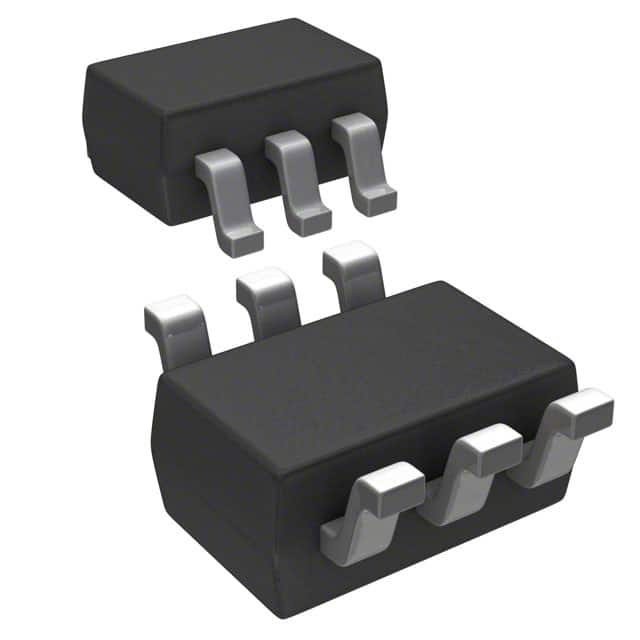
-
MCP47A1T-A0E/LT
Microchip Technology
-
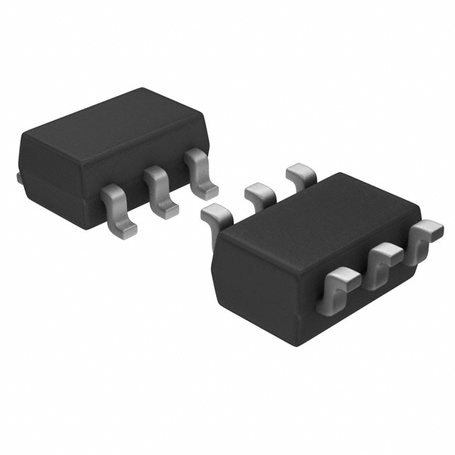
-
MCP4706A0T-E/CH
Microchip Technology
-
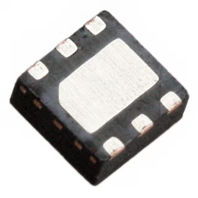
-
MCP4716A0T-E/MAY
Microchip Technology
-
-
MCP4716A0T-E/CH
Microchip Technology
-
-
MCP4726A0T-E/CH
Microchip Technology
-
-
MCP4725A0T-E/CH
Microchip Technology
-
-
MCP4725A1T-E/CH
Microchip Technology
-
-
MCP4725A2T-E/CH
Microchip Technology
-
-
MCP4726A1T-E/CH
Microchip Technology
-
-
MCP4726A3T-E/CH
Microchip Technology
-
-
MCP4726A2T-E/CH
Microchip Technology
-
-
MCP4726A0T-E/MAY
Microchip Technology
MCP4922-E/SL Sourcing & Technical Support
MCP4922-E/SL is supplied by Microchip Technology. This page provides key purchasing information including manufacturer, package, datasheet, stock reference, price reference and RFQ support.
As your reliable partner for semiconductor solutions, Flychip supports customers from research and development to mass production with electronic component supply, BOM sourcing, PCB, SMT and PCBA solutions.
Our sourcing partners include international chip manufacturers and well-known distributors. With rich experience in channel management, quality control and sales management, Flychip helps customers accelerate product development and delivery.
- Part Number
- MCP4922-E/SL
- Manufacturer
- Microchip Technology
- Package
- 14-SOIC (0.154", 3.90mm Width)
- Category
- Digital to Analog Converters (DAC)
Quick RFQ Send your inquiry and our sales team will respond quickly.
Tips
Please check your information and try again.